Low Band Frequency Synthesis
2-9
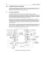
Output LOCK (U1201-4) provides information about the lock status of the synthesizer loop. A high
level at this output indicates a stable loop. A buffered output of the 16.8 MHz reference frequency is
provided at pin 19.
The operating frequency of the synthesizer is loaded serially from the microprocessor via the data
line (DATA, U1201-7), clock line (CLK, U1201-8) and chip select line (CSX, U1201-9).
The reference oscillator circuit within U1201 uses an external 16.8 MHz crystal (Y1201). Varactor
CR1201 allows software-controlled frequency adjustment (warp) and temperature compensation of
the oscillator frequency. Warp adjustment is performed using serial data from the microprocessor.
This controls the setting of an A/D converter, with its output (WARP, pin 25) applied to CR1201.
4.2
Voltage Controlled Oscillator (VCO)
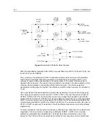
Separate VCO and buffer circuits are used for receiver injection and transmitter carrier frequency
generation. Since the receiver uses high-side injection, the receiver VCO frequency range is 10.7
MHz above the transmit VCO range. The VCO/buffers are bandsplit into three ranges depending on
radio model, covering radio operating frequencies of 29.7 to 36.0 MHz, 36.0 to 42.0 MHz, or 42.0 to
50.0 MHz. The corresponding three frequency ranges for the receive VCO are 40.4 to 46.7 MHz,
46.7 to 52.7 MHz, and 52.7 to 60.7 MHz.
The VCOs, together with Fractional-N synthesizer U1201, generate the required frequencies for
transmit and receive mode. The TRB line (U1201 pin 2) determines which VCO/buffer circuit is to be
enabled. A high level on TRB will turn on the transistors in U1378 to turn on via R1376, applying the
8.3 volt VSF source to the receiver VCO and first buffer. The second buffer in each string operates
from the 9V3 source and become active when RF is applied to their inputs.
The RF signal at the bases of the second buffers are combined and fed back to the Fractional-N
synthesizer via PRE_IN where it is compared to the reference frequency as described below in
“Synthesizer Operation”. The Fractional-N IC provides a DC steering voltage VCTRL to adjust and
maintain the VCO at the correct frequency.
With a steering voltage from 2.5V to 11V at the appropriate varactor diode (CR1302 for the RX VCO,
or CR1310 for the TX VCO), the full VCO tuning range is obtained. Each VCO uses and AGC circuit
to maintain a constant VCO output level across the frequency band. A diode (CR1306 in the receive
VCO, or CR1314 in the transmit VCO) is configured as a voltage doubler which rectifies the RF level
sampled at the VCO drain and applies a proportional negative DC voltage to the VCO gate.
Increased RF level reduces the VCO gain to compensate.
The VCO output is taken from the source and applied to the first buffer transistor (Q1304 receive,
Q1307 transmit). The first buffer output is further amplified by the second buffer transistor (Q1305
Rx, Q1308 Tx) before being applied to the receiver first mixer or transmitter first stage input.
In TX mode the modulation signal coming from the LVFRAC-N synthesizer IC (MODOUT, U1201 pin
41) is superimposed on the DC steering line voltage by capacitive divider C1215, C1208 and
C1212, causing modulation of the TX VCO using the same varactor as used for frequency control.
4.3
Synthesizer Operation
The complete synthesizer subsystem comprises mainly of low voltage LVFRAC-N synthesizer IC,
Reference Oscillator (crystal oscillator with temperature compensation), charge pump circuitry, loop
filter circuitry, and voltage-controlled oscillators and buffers. A sample of the VCO operating signal
Summary of Contents for 6864115B62-C
Page 1: ...Professional Radio GM Series Detailed Service Manual 6864115B62 C ...
Page 2: ...ii ...
Page 4: ...iv ...
Page 5: ...Professional Radio GM Series Service Maintainability Issue July 2007 ...
Page 8: ...ii ...
Page 22: ...2 10 MAINTENANCE ...
Page 25: ...Professional Radio GM Series Controlhead Service Information Issue July 2007 ...
Page 77: ...Professional Radio GM Series Controller Service Information Issue May 2007 ...
Page 100: ...2 2 TROUBLESHOOTING CHARTS ...
Page 104: ...3 4 Controller schematics parts list ...
Page 154: ...3 52 Controller T12 Schematic Diagrams ...
Page 155: ...Professional Radio GM Series VHF 136 174MHz Service Information Issue May 2007 ...
Page 164: ...1 6 MODEL CHART AND TECHNICAL SPECIFICATIONS ...
Page 176: ...2 12 THEORY OF OPERATION ...
Page 186: ...3 10 TROUBLESHOOTING CHARTS ...
Page 190: ...4 4 VHF PCB SCHEMATICS PARTS LISTS ...
Page 252: ...4 66 VHF 1 25W PCB 8471235L02 Schematics VHF 136 174 MHz IF ...
Page 256: ...4 70 VHF 1 25W PCB 8471235L02 Schematics ...
Page 257: ...Professional Radio GM Series UHF 403 470MHz Service Information Issue May 2007 ...
Page 266: ...1 6 MODEL CHART AND TECHNICAL SPECIFICATIONS ...
Page 366: ...2 12 THEORY OF OPERATION ...
Page 372: ...3 6 Low Band TROUBLESHOOTING CHARTS ...

