


UHF (403-470MHz) Transmitter Power Amplifier (PA) 40W
2-9
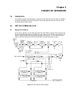
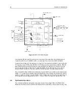
filter circuitry and DC supply. The output signal PRESC_OUT of the VCOBIC (U4301 pin12) is fed to
pin 32 of U4201 (PREIN) via a low pass filter (C4229, L4225) which attenuates harmonics and
provides the correct level to close the synthesizer loop.
The pre-scaler in the synthesizer (U4201) is basically a dual modulus pre-scaler with selectable
divider ratios. This divider ratio of the pre-scaler is controlled by the loop divider, which in turn
receives its inputs via the SRL. The output of the pre-scaler is applied to the loop divider. The output
of the loop divider is connected to the phase detector, which compares the loop divider’s output
signal with the reference signal.The reference signal is generated by dividing down the signal of the
reference oscillator (Y4261 or Y4262).
The output signal of the phase detector is a pulsed DC signal which is routed to the charge pump.
The charge pump outputs a current at pin 43 of U4201 (IOUT). The loop filter (which consists of
R4221-R4223, C4221-C4225,L4221) transforms this current into a voltage that is applied to the
varactor diodes CR4311 for transmit, CR4301, CR4302 & CR4303 for receive and alters the output
frequency of the VCO .The current can be set to a value fixed in the LVFRAC-N IC or to a value
determined by the currents flowing into BIAS 1 (U4201-40) or BIAS 2 (U4201-39). The currents are
set by the value of R4251 or R4252 respectively. The selection of the three different bias sources is
done by software programming.
To reduce synthesizer lock time when new frequency data has been loaded into the synthesizer the
magnitude of the loop current is increased by enabling the IADAPT (U4201-45) for a certain
software programmable time (Adapt Mode). The adapt mode timer is started by a low to high
transient of the CSX line. When the synthesizer is within the lock range the current is determined
only by the resistors connected to BIAS 1, BIAS 2, or the internal current source. A settled
synthesizer loop is indicated by a high level of signal LOCK (U4201-4).
The LOCK (U4201-4) signal is routed to one of the µP´s ADCs input U101-56. From the voltage the
µP determines whether LOCK is active. In order to modulate the PLL the two spot modulation
method is utilized. Via pin 10 (MODIN) on U4201 the audio signal is applied to both the A/D
converter (low freq path) as well as the balance attenuator (high freq path). The A/D converter
converts the low frequency analogue modulating signal into a digital code that is applied to the loop
divider, thereby causing the carrier to deviate. The balance attenuator is used to adjust the VCO’s
deviation sensitivity to high frequency modulating signals. The output of the balance attenuator is
present at the MODOUT port (U4201-41) and connected to the VCO modulation diode CR4321 via
R4321, C4325.
5.0
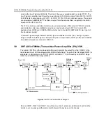
UHF (403-470MHz) Transmitter Power Amplifier (PA) 40W
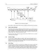
The radio’s 40 W PA is a four stage amplifier used to amplify the output from the VCOBIC to the radio
transmit level. It consists of the following four stages in the line-up. The first stage is a LDMOS
predriver (U4401) that is controlled by pin 4 of PCIC (U4501) via Q4473 (CNTLVLTG). It is followed
by another LDMOS stage (Q4421), an LDMOS stage (Q4431) and a bipolar final stage (Q4441).
Summary of Contents for 6864115B62-C
Page 1: ...Professional Radio GM Series Detailed Service Manual 6864115B62 C ...
Page 2: ...ii ...
Page 4: ...iv ...
Page 5: ...Professional Radio GM Series Service Maintainability Issue July 2007 ...
Page 8: ...ii ...
Page 22: ...2 10 MAINTENANCE ...
Page 25: ...Professional Radio GM Series Controlhead Service Information Issue July 2007 ...
Page 77: ...Professional Radio GM Series Controller Service Information Issue May 2007 ...
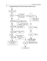
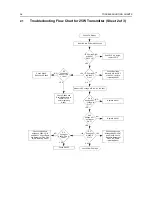
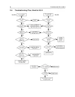
Page 100: ...2 2 TROUBLESHOOTING CHARTS ...
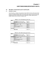
Page 104: ...3 4 Controller schematics parts list ...
Page 154: ...3 52 Controller T12 Schematic Diagrams ...
Page 155: ...Professional Radio GM Series VHF 136 174MHz Service Information Issue May 2007 ...
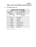
Page 164: ...1 6 MODEL CHART AND TECHNICAL SPECIFICATIONS ...
Page 176: ...2 12 THEORY OF OPERATION ...
Page 186: ...3 10 TROUBLESHOOTING CHARTS ...
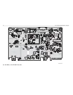
Page 190: ...4 4 VHF PCB SCHEMATICS PARTS LISTS ...
Page 252: ...4 66 VHF 1 25W PCB 8471235L02 Schematics VHF 136 174 MHz IF ...
Page 256: ...4 70 VHF 1 25W PCB 8471235L02 Schematics ...
Page 257: ...Professional Radio GM Series UHF 403 470MHz Service Information Issue May 2007 ...
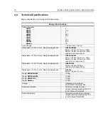
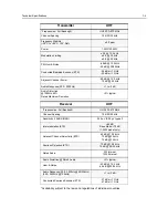
Page 266: ...1 6 MODEL CHART AND TECHNICAL SPECIFICATIONS ...
Page 366: ...2 12 THEORY OF OPERATION ...
Page 372: ...3 6 Low Band TROUBLESHOOTING CHARTS ...