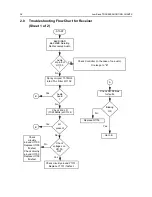
2-4
THEORY OF OPERATION
presented to the high-Q crystal filters FL1102 and FL1103, would cause ringing of the filter
response, stretching an otherwise narrow impulse into a long and audible output waveform.
Therefore, source follower stage Q1104 isolates the blanker switches from the crystal filters,
providing a consistent source impedance via matching network L1106, L1107 and associated
components. Q1104 has unity voltage gain in this configuration.
Crystal filters FL1102 and FL1103 are 2-pole, 10.7 MHz units configured to provide an overall 4-pole
response having a 3 dB bandwidth of approximately 12 kHz. The output is amplified by second IF
amplifier Q1106 and applied to the low-IF circuitry, pin 1 of IF IC (U1103). A dual hot carrier diode
(D1101) limits the amplifier output voltage swing to prevent overdriving the IF IC at RF input levels
above -27 dBm.
2.5
Low Intermediate Frequency (IF) and Receiver Back End
The 10.7 MHz high-IF signal from the second IF amplifier feeds the IF IC (U1103) at pin1. Within the
IF IC, the 10.7 MHz high -IF signal mixes with the 10.245 MHz second local oscillator (2nd LO) to
produce the low-IF signal at 455 kHz. The 2nd LO frequency is determined by crystal Y1101. The
low -IF signal is amplified and filtered by external pairs of 455 kHz ceramic filters (FL1105 and
FL1107 for 20 kHz channel spacing, or FL1104 and FL1106 for 12.5 kHz channel spacing).
Selection of the appropriate filter pair is accomplished by U1101 and U1102, controlled by the
BWSELECT line from pin 48 of the synthesizer IC U1201. The filtered output from the ceramic filters
is applied to the limiter input pin of the IF IC (pin 14).
The IF IC contains a quadrature detector using a ceramic phase-shift element (Y1102) to provide
audio detection. Internal amplification provides an audio output level of 120 mV rms (at 60%
deviation) from U1103 pin8 (AUDIOOUT) which is fed to the ASFIC_CMP (U0221) pin 2 (part of the
Controller circuitry).
A received signal strength indicator (RSSI) signal is available at U1103 pin 5, having a dynamic
range of 70 dB. The RSSI signal is interpreted by the microprocessor (U0101 pin 63) and in addition
is available at accessory connector J0501-15.
2.6
“Extender” (Noise Blanker)
The 10.7 MHz output from the first mixer, which is present at the input of first IF amp Q1101, is also
routed to the input of the “Extender” (noise blanker) circuitry and amplified by FET Q1610. The high
input impedance of the FET stage minimizes loading of the signal in the receiver path. The output of
Q1610 is further amplified by U1601, which is a wide-bandwidth, high gain differential amplifier
(used in a single-ended configuration) incorporating an AGC gain control input. This gain block
provides linear amplification of the instantaneous amplitude of the 10.7 MHz signal at the first mixer
output. The output of U1601 is coupled to biased-detector Q1603. The bias is set so that noise
impulses of a sufficient amplitude cause Q1603 to conduct. The following stages (Q1604 through
Q1606) provide additional gain and pulse shaping which slows the turn-on and turn-off waveform
applied to IF blanker switches Q1102 and Q1103. The result is that, for each noise impulse, the IF
signal is smoothly ramped off and then on again, preventing the pulse from reaching the narrow IF
selectivity, where ringing would cause an objectionable spike at the detector of a much longer
duration than the original impulse.
If the repetition rate of noise impulses is so rapid that the noise blanker can no longer blank them
individually, as indicated by a large increase in high-frequency content at the output of Q1604, stage
Q1607 amplifies this level and turns on level detector Q1609. Its output is highly filtered into a DC
voltage level which is proportional to the repetition rate of the noise impulses, and this is applied to
Summary of Contents for 6864115B62-C
Page 1: ...Professional Radio GM Series Detailed Service Manual 6864115B62 C ...
Page 2: ...ii ...
Page 4: ...iv ...
Page 5: ...Professional Radio GM Series Service Maintainability Issue July 2007 ...
Page 8: ...ii ...
Page 22: ...2 10 MAINTENANCE ...
Page 25: ...Professional Radio GM Series Controlhead Service Information Issue July 2007 ...
Page 77: ...Professional Radio GM Series Controller Service Information Issue May 2007 ...
Page 100: ...2 2 TROUBLESHOOTING CHARTS ...
Page 104: ...3 4 Controller schematics parts list ...
Page 154: ...3 52 Controller T12 Schematic Diagrams ...
Page 155: ...Professional Radio GM Series VHF 136 174MHz Service Information Issue May 2007 ...
Page 164: ...1 6 MODEL CHART AND TECHNICAL SPECIFICATIONS ...
Page 176: ...2 12 THEORY OF OPERATION ...
Page 186: ...3 10 TROUBLESHOOTING CHARTS ...
Page 190: ...4 4 VHF PCB SCHEMATICS PARTS LISTS ...
Page 252: ...4 66 VHF 1 25W PCB 8471235L02 Schematics VHF 136 174 MHz IF ...
Page 256: ...4 70 VHF 1 25W PCB 8471235L02 Schematics ...
Page 257: ...Professional Radio GM Series UHF 403 470MHz Service Information Issue May 2007 ...
Page 266: ...1 6 MODEL CHART AND TECHNICAL SPECIFICATIONS ...
Page 366: ...2 12 THEORY OF OPERATION ...
Page 372: ...3 6 Low Band TROUBLESHOOTING CHARTS ...

