


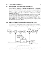


VHF (136-174MHz) Transmitter Power Amplifier (PA) 25 W
2-5
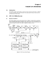
3.4
Directional Coupler
The directional coupler is a microstrip printed circuit, which couples a small amount of the forward
power delivered by Q3441. The coupled signal is rectified by D3451. The DC voltage is proportional
to the RF output power and feeds the RFIN port of the PCIC (U3501 pin 1). The PCIC controls the
gain of stage U3401 and Q3421 as necessary to hold this voltage constant, thus ensuring the
forward power out of the radio to be held to a constant value.
3.5
Antenna Switch
The antenna switch consists of two PIN diodes, D3471 and D3472. In the receive mode, both diodes
are off. Signals applied at the antenna jack J3401 are routed, via the harmonic filter, through
network L3472, C3474 and C3475, to the receiver input. In the transmit mode, K9V1 turns on
Q3471 which enables current sink Q3472, set to 96 mA by R3473 and VR3471. This completes a
DC path from PASUPVLTG, through L3437, D3471, L3472, D3472, L3471, R3474 and the current
sink, to ground. Both diodes are forward biased into conduction. The transmitter RF from the
directional coupler is routed via D3471 to the harmonic filter and antenna jack. D3472 also
conducts, shunting RF power and preventing it from reaching the receiver port (RXIN). L3472 is
selected to appear as a lambda / 4 wave transmission line, making the short circuit presented by
D3472 appear as an open circuit at the junction of D3472 and the receiver path.
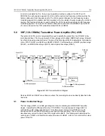
3.6
Harmonic Filter
Components L3491-L3493 and L3472, C3491-C3499 form a Chebychev low-pass filter to attenuate
harmonic energy of the transmitter to specifications level. R3491 is used to drain electrostatic
charge that might otherwise build up on the antenna. The harmonic filter also prevents high level RF
signals above the receiver passband from reaching the receiver circuits, improving spurious
response rejection.
3.7
Power Control
The transmitter uses the Power Control IC (PCIC, U3501) to control the power output of the radio. A
portion of the forward RF power from the transmitter is sampled by the directional coupler and
rectified, to provide a DC voltage to the RFIN port of the PCIC (pin 1) which is proportional to the
sampled RF power.
The ASFIC (U0221) has internal digital to analog converters (DACs) which provide a reference
voltage of the control loop to the PCIC via R3505. The reference voltage level is programmable
through the SPI line of the PCIC. This reference voltage is proportional to the desired power setting
of the transmitter, and is factory programmed at several points across the frequency range of the
transmitter to offset frequency response variations of the transmitter’s power detector circuit.
The PCIC provides a DC output voltage at pin 4 (INT) which sets the drain current of the first
(U3401) and second (Q3421) transmitter stage via current control op-amps U3402-1 and U3402-2.
This adjusts the transmitter power output to the intended value. Variations in forward transmitter
power cause the DC voltage at pin 1 to change, and the PCIC adjusts the control voltage above or
below its nominal value to raise or lower output power. Capacitors C3502-4, in conjunction with
resistors and integrators within the PCIC, control the transmitter power-rise (key-up) and power-
decay (de-key) characteristic to minimize splatter into adjacent channels. U3502 is a temperature-
sensing device, which monitors the circuit board temperature in the vicinity of the transmitter driver
and final devices, and provides a dc voltage to the PCIC (TEMP, pin 30) proportional to temperature.
If the DC voltage produced exceeds the set threshold in the PCIC, the transmitter output power will
be reduced so as to reduce the transmitter temperature.
Summary of Contents for 6864115B62-C
Page 1: ...Professional Radio GM Series Detailed Service Manual 6864115B62 C ...
Page 2: ...ii ...
Page 4: ...iv ...
Page 5: ...Professional Radio GM Series Service Maintainability Issue July 2007 ...
Page 8: ...ii ...
Page 22: ...2 10 MAINTENANCE ...
Page 25: ...Professional Radio GM Series Controlhead Service Information Issue July 2007 ...
Page 77: ...Professional Radio GM Series Controller Service Information Issue May 2007 ...
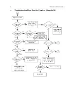
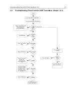
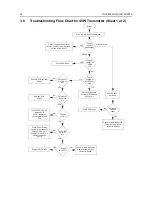
Page 100: ...2 2 TROUBLESHOOTING CHARTS ...
Page 104: ...3 4 Controller schematics parts list ...
Page 154: ...3 52 Controller T12 Schematic Diagrams ...
Page 155: ...Professional Radio GM Series VHF 136 174MHz Service Information Issue May 2007 ...
Page 164: ...1 6 MODEL CHART AND TECHNICAL SPECIFICATIONS ...
Page 176: ...2 12 THEORY OF OPERATION ...
Page 186: ...3 10 TROUBLESHOOTING CHARTS ...
Page 190: ...4 4 VHF PCB SCHEMATICS PARTS LISTS ...
Page 252: ...4 66 VHF 1 25W PCB 8471235L02 Schematics VHF 136 174 MHz IF ...
Page 256: ...4 70 VHF 1 25W PCB 8471235L02 Schematics ...
Page 257: ...Professional Radio GM Series UHF 403 470MHz Service Information Issue May 2007 ...
Page 266: ...1 6 MODEL CHART AND TECHNICAL SPECIFICATIONS ...
Page 366: ...2 12 THEORY OF OPERATION ...
Page 372: ...3 6 Low Band TROUBLESHOOTING CHARTS ...