


2-6
THEORY OF OPERATION
4.0
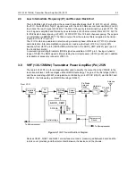
VHF (136-174MHz) Frequency Synthesis
The frequency synthesizer subsystem consists of the reference oscillator (Y3261 or Y3263), the
Low Voltage Fractional-N synthesizer (LVFRAC-N, U3201), and the voltage-controlled oscillators
and buffer amplifiers (U3301, Q3301-2 and associated circuitry).
4.1
Reference Oscillator
The reference oscillator (Y3263) contains a temperature compensated crystal oscillator with a
frequency of 16.8 MHz. An analog to digital (A/D) converter internal to U3201 (LVFRAC-N) and
controlled by the microprocessor via serial interface (SRL) sets the voltage at the warp output of
U3201 (pin 25) to set the frequency of the oscillator. The output of the oscillator (U3263 pin 3) is
applied to pin 23 (XTAL1) of U3201 via R3263 and C3235.
In applications were less frequency stability is required, the oscillator inside U3201 is used along
with an external crystal Y3261, varactor diode D3261, C3261, C3262 and R3262. In this case,
Y3263, R3263, C3235 and C3251 are not used. When Y3263 is used, Y3261, D3261, C3261,
C3262 and R3262 are not used, and C3263 is increased to 0.1 uF.
4.2
Fractional-N Synthesizer
The LVFRAC-N synthesizer IC (U3201) consists of a pre-scaler, a programmable loop divider,
control divider logic, a phase detector, a charge pump, an A/D converter for low frequency digital
modulation, a balance attenuator to balance the high frequency analog modulation and low
frequency digital modulation, a 13V positive voltage multiplier, a serial interface for control, and
finally a super filter for the regulated 5 volts.
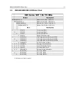
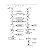
Figure 3-1
VHF Synthesizer Block Diagram
DATA
CLK
CEX
MODIN
VCC, DC5V
XTAL1
XTAL2
WARP
PREIN
VCP
REFERENCE
OSCILLATOR
VOLTAGE
MULTIPLIER
DATA (U0101 PIN 100)
CLOCK (U0101 PIN 1)
CSX (U0101 PIN 2)
MOD IN (U0221 PIN 40)
+5V (U3211 PIN 1)
7
8
9
10
13, 30
23
24
25
32
47
VMULT2
VMULT1
BIAS1
SFOUT
AUX3
AUX4
IADAPT
IOUT
GND
FREFOUT
LOCK
4
19
6, 22, 33, 44
43
45
3
2
28
14
15
40
FILTERED 5V
STEERING
LOCK (U0101 PIN 56)
PRESCALER IN
FREF (U0221 PIN 34)
39
BIAS2
41
48
5, 20, 34, 36
+5V (U3211 PIN 1)
AUX1
VDD, DC5V
MODOUT
U3201
LOW VOLTAGE
FRACTIONAL-N
SYNTHESIZER
AUX2
BW SELECT
TX RF INJECTION
(1ST STAGE OF PA)
LO RF INJECTION
VOLTAGE
CONTROLLED
OSCILLATOR
LINE
2-POLE
LOOP
FILTER
1
TRB
TO IF SECTION
Summary of Contents for 6864115B62-C
Page 1: ...Professional Radio GM Series Detailed Service Manual 6864115B62 C ...
Page 2: ...ii ...
Page 4: ...iv ...
Page 5: ...Professional Radio GM Series Service Maintainability Issue July 2007 ...
Page 8: ...ii ...
Page 22: ...2 10 MAINTENANCE ...
Page 25: ...Professional Radio GM Series Controlhead Service Information Issue July 2007 ...
Page 77: ...Professional Radio GM Series Controller Service Information Issue May 2007 ...
Page 100: ...2 2 TROUBLESHOOTING CHARTS ...
Page 104: ...3 4 Controller schematics parts list ...
Page 154: ...3 52 Controller T12 Schematic Diagrams ...
Page 155: ...Professional Radio GM Series VHF 136 174MHz Service Information Issue May 2007 ...
Page 164: ...1 6 MODEL CHART AND TECHNICAL SPECIFICATIONS ...
Page 176: ...2 12 THEORY OF OPERATION ...
Page 186: ...3 10 TROUBLESHOOTING CHARTS ...
Page 190: ...4 4 VHF PCB SCHEMATICS PARTS LISTS ...
Page 252: ...4 66 VHF 1 25W PCB 8471235L02 Schematics VHF 136 174 MHz IF ...
Page 256: ...4 70 VHF 1 25W PCB 8471235L02 Schematics ...
Page 257: ...Professional Radio GM Series UHF 403 470MHz Service Information Issue May 2007 ...
Page 266: ...1 6 MODEL CHART AND TECHNICAL SPECIFICATIONS ...
Page 366: ...2 12 THEORY OF OPERATION ...
Page 372: ...3 6 Low Band TROUBLESHOOTING CHARTS ...