2-10
THEORY OF OPERATION
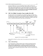
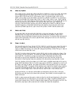
In receive mode the voltage control line is at ground level and turns off Q3501-2, which in turn
switches off the biasing voltage to U3401.
5.2
Pre-Driver Stage
The next stage is an LDMOS device (Q3421) providing a gain of 13 dB. This device requires a
positive gate bias and a quiescent current flow for proper operation. The voltage of the line
PCIC_MOSBIAS_1 is set during transmit mode by the PCIC pin 24, and fed to the gate of Q3421
via the resistive network R3410, R3415, and R3416. The bias voltage is tuned in the factory.
5.3
Driver Stage
The following stage is an enhancement-mode N-Channel MOSFET device (Q3431) providing a gain
of 10dB. This device also requires a positive gate bias and a quiescent current flow for proper
operation. The voltage of the line MOSBIAS_2 is set in transmit mode by the ASFIC and fed to the
gate of Q3431 via the resistive network R3404, R3406, and R3431-5. This bias voltage is also tuned
in the factory. If the transistor is replaced, the bias voltage must be tuned using the Customer
Programming Software (CPS). Care must be taken not to damage the device by exceeding the
maximum allowed bias voltage. The device’s drain current is drawn directly from the radio’s DC
supply voltage input, PASUPVLTG, via L3431 and L3432.
5.4
Final Stage
The final stage uses the bipolar device Q3441. The device’s collector current is also drawn from the
radio’s DC supply voltage input. To maintain class C operation, the base is DC-grounded by a series
inductor (L3441) and a bead (L3442). A matching network consisting of C3446-52, C3467, L3444-5,
and two striplines, transforms the impedance to approximately 50 ohms and feeds the directional
coupler.
5.5
Directional Coupler
The directional coupler is a microstrip printed circuit, which couples a small amount of the forward
and reflected power delivered by Q3441. The coupled signals are rectified by D3451-2 and
combined by R3463-4. The resulting DC voltage is proportional to RF output power and feeds the
RFIN port of the PCIC (U3501 pin 1). The PCIC controls the gain of stage U3401 as necessary to
hold this voltage constant, thus ensuring the forward power out of the radio to be held to a constant
value.
An abnormally high reflected power level, such as may be caused by a damaged antenna, also
causes the DC voltage applied to the PCIC to increase, and this will cause a reduction in the gain of
U3401, reducing transmitter output power to prevent damage to the final device due to an improper
load.
Summary of Contents for 6864115B62-C
Page 1: ...Professional Radio GM Series Detailed Service Manual 6864115B62 C ...
Page 2: ...ii ...
Page 4: ...iv ...
Page 5: ...Professional Radio GM Series Service Maintainability Issue July 2007 ...
Page 8: ...ii ...
Page 22: ...2 10 MAINTENANCE ...
Page 25: ...Professional Radio GM Series Controlhead Service Information Issue July 2007 ...
Page 77: ...Professional Radio GM Series Controller Service Information Issue May 2007 ...
Page 100: ...2 2 TROUBLESHOOTING CHARTS ...
Page 104: ...3 4 Controller schematics parts list ...
Page 154: ...3 52 Controller T12 Schematic Diagrams ...
Page 155: ...Professional Radio GM Series VHF 136 174MHz Service Information Issue May 2007 ...
Page 164: ...1 6 MODEL CHART AND TECHNICAL SPECIFICATIONS ...
Page 176: ...2 12 THEORY OF OPERATION ...
Page 186: ...3 10 TROUBLESHOOTING CHARTS ...
Page 190: ...4 4 VHF PCB SCHEMATICS PARTS LISTS ...
Page 252: ...4 66 VHF 1 25W PCB 8471235L02 Schematics VHF 136 174 MHz IF ...
Page 256: ...4 70 VHF 1 25W PCB 8471235L02 Schematics ...
Page 257: ...Professional Radio GM Series UHF 403 470MHz Service Information Issue May 2007 ...
Page 266: ...1 6 MODEL CHART AND TECHNICAL SPECIFICATIONS ...
Page 366: ...2 12 THEORY OF OPERATION ...
Page 372: ...3 6 Low Band TROUBLESHOOTING CHARTS ...

