


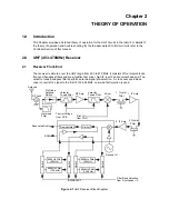
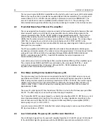


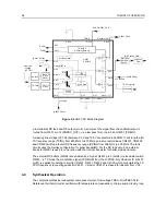


UHF (403-470MHz) Frequency Synthesis
2-7
Figure 2-3
UHF Synthesizer Block Diagram
A voltage of 5V applied to the super filter input (U4201 pin 30) supplies an output voltage of 4.5
VDC(VSF) at pin 28. It supplies the VCO, VCO modulation bias circuit (via R4322) and the
synthesizer charge pump resistor network (R4251, R4252). The synthesizer supply voltage is
provided by the 5V regulator U4211.
In order to generate a high voltage to supply the phase detector (charge pump) output stage at pin
VCP (U4201-47), a voltage of 13 VDC is being generated by the positive voltage multiplier circuitry
(D4201, C4202, C4203). This voltage multiplier is basically a diode capacitor network driven by two
(1.05MHz) 180 degrees out of phase signals (U4201-14 and -15).
Output LOCK (U4201-4) provides information about the lock status of the synthesizer loop. A high
level at this output indicates a stable loop. IC U4201 provides the 16.8 MHz reference frequency at
pin 19.
The serial interface (SRL) is connected to the microprocessor via the data line DATA (U4201-7),
clock line CLK (U4201-8), and chip enable line CSX (U4201-9).
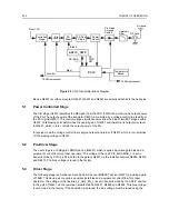
4.3
Voltage Controlled Oscillator (VCO)
The Voltage Controlled Oscillator (VCO) consists of the VCO/Buffer IC (VCOBIC, U4301), the TX
and RX tank circuits, the external RX buffer stages, and the modulation circuitry.
The VCOBIC together with Fractional-N synthesizer (U4201) generates the required frequencies in
both transmit and receive modes. The TRB line (U4301 pin 19) determines which tank circuits and
internal buffers are to be enabled. A high level on TRB enables TX tank and TX output (pin 10), and
DATA
CLK
CEX
MODIN
VCC, DC5V
XTAL1
XTAL2
WARP
PREIN
VCP
REFERENCE
OSCILLATOR
VOLTAGE
MULTIPLIER
DATA (U0101 PIN 100)
CLOCK (U0101 PIN 1)
CSX (U0101 PIN 2)
MOD IN (U0221 PIN 40)
+5V (U4211 PIN 1)
7
8
9
10
13, 30
23
24
25
32
47
VMULT2
VMULT1
BIAS1
SFOUT
AUX3
AUX4
IADAPT
IOUT
GND
FREFOUT
LOCK
4
19
6, 22, 33, 44
43
45
3
2
28
14
15
40
FILTERED 5V
STEERING
LOCK (U0101 PIN 56)
PRESCALER IN
FREF (U0221 PIN 34)
39
BIAS2
41
48
5, 20, 34, 36
+5V (U4211 PIN 1)
AUX1
VDD, DC5V
MODOUT
U4201
LOW VOLTAGE
FRACTIONAL-N
SYNTHESIZER
AUX2
1 (NU)
BWSELECT
VCO Bias
TRB
To IF
Section
TX RF INJECTION
(1ST STAGE OF PA)
LO RF INJECTION
VOLTAGE
CONTROLLED
OSCILLATOR
LINE
2-POLE
LOOP
FILTER
Summary of Contents for 6864115B62-C
Page 1: ...Professional Radio GM Series Detailed Service Manual 6864115B62 C ...
Page 2: ...ii ...
Page 4: ...iv ...
Page 5: ...Professional Radio GM Series Service Maintainability Issue July 2007 ...
Page 8: ...ii ...
Page 22: ...2 10 MAINTENANCE ...
Page 25: ...Professional Radio GM Series Controlhead Service Information Issue July 2007 ...
Page 77: ...Professional Radio GM Series Controller Service Information Issue May 2007 ...
Page 100: ...2 2 TROUBLESHOOTING CHARTS ...
Page 104: ...3 4 Controller schematics parts list ...
Page 154: ...3 52 Controller T12 Schematic Diagrams ...
Page 155: ...Professional Radio GM Series VHF 136 174MHz Service Information Issue May 2007 ...
Page 164: ...1 6 MODEL CHART AND TECHNICAL SPECIFICATIONS ...
Page 176: ...2 12 THEORY OF OPERATION ...
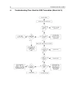
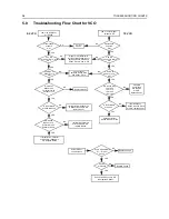
Page 186: ...3 10 TROUBLESHOOTING CHARTS ...
Page 190: ...4 4 VHF PCB SCHEMATICS PARTS LISTS ...
Page 252: ...4 66 VHF 1 25W PCB 8471235L02 Schematics VHF 136 174 MHz IF ...
Page 256: ...4 70 VHF 1 25W PCB 8471235L02 Schematics ...
Page 257: ...Professional Radio GM Series UHF 403 470MHz Service Information Issue May 2007 ...
Page 266: ...1 6 MODEL CHART AND TECHNICAL SPECIFICATIONS ...
Page 366: ...2 12 THEORY OF OPERATION ...
Page 372: ...3 6 Low Band TROUBLESHOOTING CHARTS ...