2-4
THEORY OF OPERATION
3.1
First Power Controlled Stage
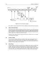
The first stage (U4401) is a 20dB gain integrated circuit containing two LDMOS FET amplifier
stages. It amplifies the RF signal from the VCO (TXINJ). The output power of stage U4401 is
controlled by a DC voltage applied to pin 1 from the op-amp U4402-1, pin 1. The control voltage
simultaneously varies the bias of two FET stages within U4401. This biasing point determines the
overall gain of U4401 and therefore its output drive level to Q4421, which in turn controls the output
power of the PA.
Op-amp U4402-1 monitors the drain current of U4401 via resistor R4444 and adjusts the bias
voltage of U4401 so that the current remains constant. The PCIC (U4501) provides a DC output
voltage at pin 4 (INT) which sets the reference voltage of the current control loop. A raising power
output causes the DC voltage from the PCIC to fall, and U4402-1 adjusts the bias voltage for a
lower drain current to lower the gain of the stage.
In receive mode the DC voltage from PCIC pin 23 (RX) turns on Q4442, which in turn switches off
the biasing voltage to U4401.
Switch S5440 is a pressure pad with a conductive strip which connects two conductive areas on the
board when the radio's cover is properly screwed to the chassis. When the cover is removed, S5440
opens and the resulting high voltage level at the inverting inputs of the current control op-amps
U4402-1 & 2 switches off the biasing of U4401 and Q4421. This prevents transmitter key up while
the devices do not have proper thermal contact to the chassis.
3.2
Power Controlled Driver Stage
The next stage is an LDMOS device (Q4421) providing a gain of 12dB. This device requires a
positive gate bias and a quiescent current flow for proper operation. The bias is set during transmit
mode by the drain current control op-amp U4402-2, and fed to the gate of Q4421 via the resistive
network R4429, R4418, R4415 and R4416.
Op-amp U4402-2 monitors the drain current of U4421 via resistors R4424-27 and adjusts the bias
voltage of Q4421 so that the current remains constant. The PCIC (U4501) provides a DC output
voltage at pin 4 (INT) which sets the reference voltage of the current control loop. A raising power
output causes the DC voltage from the PCIC to fall, and U4402-2 adjusts the bias voltage for a
lower drain current to lower the gain of the stage.
In receive mode the DC voltage from PCIC pin 23 (RX) turns on Q4422, which in turn switches off
the biasing voltage to Q4421.
3.3
Final Stage
The final stage is an LDMOS device (Q4441) providing a gain of 12dB. This device also requires a
positive gate bias and a quiescent current flow for proper operation. The voltage of the line
MOSBIAS_2 is set in transmit mode by the ASFIC and fed to the gate of Q4441 via the resistive
network R4404, R4406, and R4431-2. This bias voltage is tuned in the factory. If the transistor is
replaced, the bias voltage must be tuned using the Golbal Tuner. Care must be taken not to
damage the device by exceeding the maximum allowed bias voltage. The device’s drain current is
drawn directly from the radio’s DC supply voltage input, PASUPVLTG, via L4436 and L4437.
A matching network consisting of C4441-49 and striplines transforms the impedance to 50 ohms
and feeds the directional coupler.
Summary of Contents for 6864115B62-C
Page 1: ...Professional Radio GM Series Detailed Service Manual 6864115B62 C ...
Page 2: ...ii ...
Page 4: ...iv ...
Page 5: ...Professional Radio GM Series Service Maintainability Issue July 2007 ...
Page 8: ...ii ...
Page 22: ...2 10 MAINTENANCE ...
Page 25: ...Professional Radio GM Series Controlhead Service Information Issue July 2007 ...
Page 77: ...Professional Radio GM Series Controller Service Information Issue May 2007 ...
Page 100: ...2 2 TROUBLESHOOTING CHARTS ...
Page 104: ...3 4 Controller schematics parts list ...
Page 154: ...3 52 Controller T12 Schematic Diagrams ...
Page 155: ...Professional Radio GM Series VHF 136 174MHz Service Information Issue May 2007 ...
Page 164: ...1 6 MODEL CHART AND TECHNICAL SPECIFICATIONS ...
Page 176: ...2 12 THEORY OF OPERATION ...
Page 186: ...3 10 TROUBLESHOOTING CHARTS ...
Page 190: ...4 4 VHF PCB SCHEMATICS PARTS LISTS ...
Page 252: ...4 66 VHF 1 25W PCB 8471235L02 Schematics VHF 136 174 MHz IF ...
Page 256: ...4 70 VHF 1 25W PCB 8471235L02 Schematics ...
Page 257: ...Professional Radio GM Series UHF 403 470MHz Service Information Issue May 2007 ...
Page 266: ...1 6 MODEL CHART AND TECHNICAL SPECIFICATIONS ...
Page 366: ...2 12 THEORY OF OPERATION ...
Page 372: ...3 6 Low Band TROUBLESHOOTING CHARTS ...


