


Power Line Carrier ____________________________________________________________________
RF-MCGARDPRO
Hubbell Power Systems, Inc.
–
RFL™
Products
July 1, 2022
©2022 Hubbell Incorporated
5-54
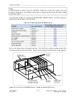
Figure 5-33. 50W Power Amp Circuit Board
Two DIP Switch banks SW1 and SW2 have been added to the Power Amp Circuit Board. These
switches are factory set for optimum operation but can be changed in the field if required. The
DIP switches shown above are factory set to protect the circuit board from overvoltage or
excessive phase angle situations. See
for a description of the switch settings.
If the protective circuits are activated the Power Amplifier will shut down for approximately 2.5
seconds and then come up for 25ms. This pattern will continue until the safety parameters are
met and the condition cleared.
Table 5-21 Function of the Jumpers, Connectors and Potentiometers on the Power Amp Circuit Board
Reference
Designation
Component
Function
DS1
LED (green)
This LED is located on the front left panel of the Power Amplifier.
The LED is lit when the Power Amplifier is transmitting.
J1
connector
Provides input dc voltage from power supply, +92Vdc and +30Vdc.
J2
connector
Power output to TX Filter Module.
J3
connector
Power amplifier failure alarm output signal. Signal goes to alarm
relay on balance board, which provides form-C contacts on back of
RF chassis. Output is +12Vdc when power amp fails.
J4
connector
TX In (RF input signal from back of MA-650)
J5
connector
Spare TX In (not used)


