MC96FM204/FM214
April 7, 2016 Ver. 1.8
37
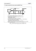
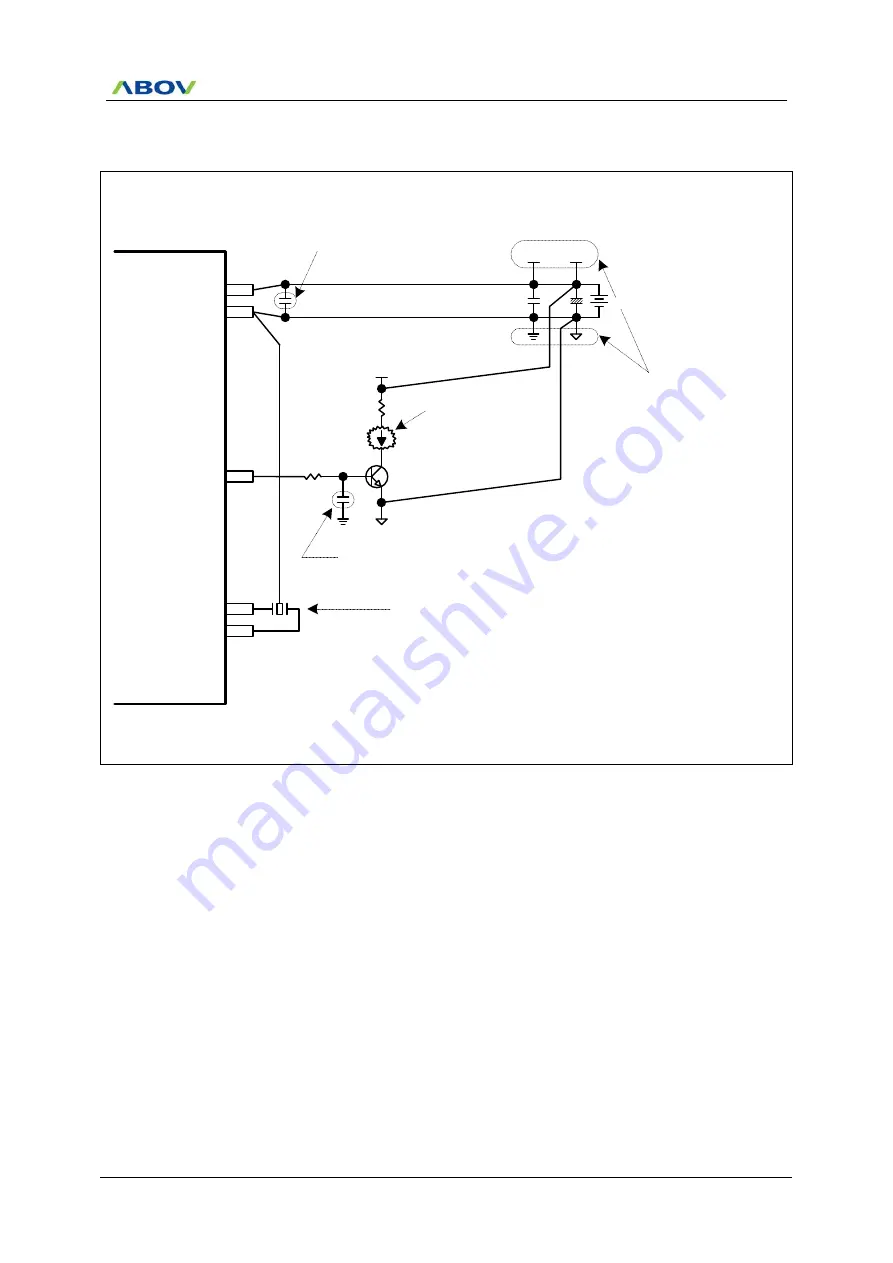
7.20 Recommended Circuit and Layout
{
}
M
C
9
6
F
M
2
0
4
/F
M
2
1
4
XOUT
XIN
I/O
VSS
VDD
High-Current Part
Infrared LED,
FND(7-Segment),
,,,,,
etc
{ }
0.01uF
VCC
0.1uF
This 0.1uF capacitor should be within
1cm from the VDD pin of MCU on the
PCB layout.
{
}
This 0.01uF capacitor is alternatively
for noise immunity.
X-tal
The main crystal should be as close
by the MCU as possible.
+
0.1uF
VDD
VCC
{
}
The MCU power line (VDD and VSS)
should be separated from the high-
current part at a DC power node on
the PCB layout.
DC Power
Figure 7.9 Recommended Circuit and Layout
Summary of Contents for MC96FM204
Page 17: ...MC96FM204 FM214 April 7 2016 Ver 1 8 17 4 Package Diagram Figure 4 1 20 Pin SOP Package ...
Page 18: ...MC96FM204 FM214 18 April 7 2016 Ver 1 8 Figure 4 2 20 Pin TSSOP Package ...
Page 19: ...MC96FM204 FM214 April 7 2016 Ver 1 8 19 Figure 4 3 16 Pin SOP Package ...
Page 20: ...MC96FM204 FM214 20 April 7 2016 Ver 1 8 Figure 4 4 16 Pin TSSOP Package ...


