MC96FM204/FM214
22
April 7, 2016 Ver. 1.8
Table 5-1 Normal pin description (Continued)
PIN
Name
I/O
Function
@RESET
Shared with
AN0
I/O A/D converter analog input channels
Input
P04/MOSI/OP1IN
AN1
P05/OP0OUT
AN2
P06/OP0N
AN3
P07/OP0P
AN4
P10/CMP-/EINT0
AN5
P11/CMP+/EINT1
AN6
P12/CMPO/BUZO
AN7
Output
P13/EINT2
DSDA
I/O On chip debugger data input/output
(NOTE4,5)
Input
P20
DSCL
I/O On chip debugger clock input
(NOTE4, 5)
Input
P21
CMPO
I/O Analog comparator output.
The CMPO is only in MC96FM204D/R/M/H device.
Input
P12/AN6/BUZO
CMP-
I/O Analog comparator negative input.
The CMP- is only in MC96FM204D/R/M/H device.
Input
P10/AN4/EINT0
CMP+
I/O Analog comparator positive input.
The CMP+ is only in MC96FM204D/R/M/H device.
Input
P11/AN5/EINT1
OP0P
I/O OP-AMP 0 positive input.
The OP0P is only in MC96FM204D/R/M/H device.
Input
P07/AN3
OP0N
I/O OP-AMP 0 negative input.
The OP0N is only in MC96FM204D/R/M/H device.
Input
P06/AN2
OP0OUT
I/O OP-AMP 0 output.
The OP0OUT is only in MC96FM204D/R/M/H device.
Input
P05/AN1
OP1IN
I/O OP-AMP 1 input.
The OP1IN is only in MC96FM204D/R/M/H device.
Input
P04/AN0/MOSI
RESETB
I/O System reset pin with a pull-up resistor when it is
selected as the RESETB by CONFIGURE OPTION 2
Input
P01/SS/EC1
XIN
I/O Main oscillator pins
Input
P03/MISO
XOUT
P02/SCK
AVSS
–
A/D converter and OP-AMP ground.
The AVSS is only in MC96FM204D/R/M/H device.
–
–
VDD,
VSS
–
Power input pins
–
–
NOTES) 1. The P14
– P16 are only in the 20-pin package.
2. The P13 is in the 20-pin and 16-pin(without OP-AMP) package.
3.
The P01/RESETB/SS/EC1 is configured as one of the P01/SS/EC1 and the RESETB pin by the
“CONFIGURE OPTION 2”.
4. If the P20/DSDA and P21/DSCL pins are connected to an emulator during reset or power-on reset,
the pins are automatically configured as the debugger pins.
5. The P20/DSDA and P21/DSCL pins are configured as inputs with internal pull-up resistor
only during the reset or power-on reset.
6. The P03/XIN/MISO and P02/XOUT/SCK are configured as a function pin by software control.
Summary of Contents for MC96FM204
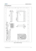
Page 17: ...MC96FM204 FM214 April 7 2016 Ver 1 8 17 4 Package Diagram Figure 4 1 20 Pin SOP Package ...
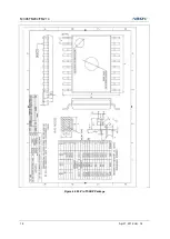
Page 18: ...MC96FM204 FM214 18 April 7 2016 Ver 1 8 Figure 4 2 20 Pin TSSOP Package ...
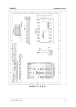
Page 19: ...MC96FM204 FM214 April 7 2016 Ver 1 8 19 Figure 4 3 16 Pin SOP Package ...
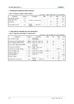
Page 20: ...MC96FM204 FM214 20 April 7 2016 Ver 1 8 Figure 4 4 16 Pin TSSOP Package ...


