MC96FM204/FM214
April 7, 2016 Ver. 1.8
87
11.4 Timer 0
11.4.1 Overview
The 8-bit timer 0 consists of multiplexer, timer 0 counter register, timer 0 data register and timer 0 control
register (T0CNT, T0DR, T0CR).
-
8-bit timer/counter mode
The timer/counter 0 can be clocked by an internal clock source. The clock source is selected by clock selection
logic which is controlled by the clock selection bits (T0CK[2:0]).
- TIMER0 clock source: f
X
/1, 4, 16, 64, 256, 1024, 4096
11.4.2 8-Bit Timer/Counter Mode
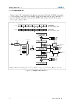
The 8-bit timer/counter mode is selected by control register as shown in Figure 11.5.
The 8-bit timer have counter and data register. The counter register is increased by internal clock input. Timer 0
can use the input clock with one of 1, 4, 16, 64, 256, 1024 and 4096 prescaler division rates (T0CK[2:0]). When
the value of T0CNT and T0DR is identical in timer 0, a match signal is generated and the interrupt of Timer 0
occurs. T0CNT value is automatically cleared by match signal. It can be also cleared by software (T0CC).
P
r
e
s
c
a
l
e
r
fx
M
U
X
fx/4
fx/16
fx/256
fx/1024
fx/4096
fx/64
3
T0CK[2:0]
T0EN
8-bit Counter
Comparator
8-bit Data Register
T0 (8Bit)
T0DR (8Bit)
MSB
LSB
MSB
LSB
T0IFR
INT_ACK
Clear
fx/1
To interrupt
block
T0CC
Clear
Match signal
Match
T0EN
T0CR
1
ADDRESS:B2H
INITIAL VALUE : 0000_0000B
–
–
T0IFR
T0CK2
T0CK1
T0CK0
T0CC
–
–
X
X
X
X
X
Figure 11.5 8-Bit Timer/Counter Mode for Timer 0
Summary of Contents for MC96FM204
Page 17: ...MC96FM204 FM214 April 7 2016 Ver 1 8 17 4 Package Diagram Figure 4 1 20 Pin SOP Package ...
Page 18: ...MC96FM204 FM214 18 April 7 2016 Ver 1 8 Figure 4 2 20 Pin TSSOP Package ...
Page 19: ...MC96FM204 FM214 April 7 2016 Ver 1 8 19 Figure 4 3 16 Pin SOP Package ...
Page 20: ...MC96FM204 FM214 20 April 7 2016 Ver 1 8 Figure 4 4 16 Pin TSSOP Package ...

