MC96FM204/FM214
96
April 7, 2016 Ver. 1.8
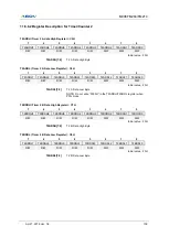
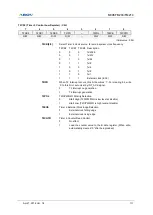
11.5.4 16-Bit PPG Mode
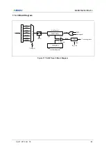
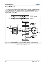
The timer 1 has a PPG (Programmable Pulse Generation) function. In PPG mode, T1O/PWM1O pin outputs
up to 16-bit resolution PWM output. This pin should be configured as a PWM output by setting PFSRL00
to ‘1’ .
The period of the PWM output is determined by the T1ADRH/T1ADRL. And the duty of the PWM output is
determined by the T1BDRH/T1BDRL.
T1MS[1:0]
T1POL
Reload
A Match
T1CC
T1EN
P
r
e
s
c
a
l
e
r
fx
M
U
X
fx/2
fx/4
fx/64
fx/512
fx/2048
fx/8
fx/1
Comparator
16-bit Counter
T1CNTH/T1CNTL
16-bit B Data Register
T1BDRH/T1BDRL
Clear
B Match
Edge
Detector
T1ECE
EC1
Buffer Register B
Comparator
16-bit A Data Register
T1ADRH/T1ADRL
T1IFR
INT_ACK
Clear
To interrupt
block
A Match
Buffer Register A
Reload
Pulse
Generator
T1O/
PWM1O
R
T1EN
3
T1CK[2:0]
2
T1EN
T1CRH
1
ADDRESS:BBH
INITIAL VALUE : 0000_0000B
–
T1MS1
T1MS0
–
–
–
T1CC
–
1
1
–
–
–
X
T1CK2
T1CRL
X
ADDRESS:BAH
INITIAL VALUE : 0000_0000B
T1CK1
T1CK0
T1IFR
–
T1POL
T1ECE T1CNTR
X
X
X
–
X
X
X
A Match
T1CC
T1EN
A Match
T1CC
T1EN
NOTE) The T1EN is automatically cleared to logic
“0” after one pulse is generated at a PPG one-shot mode.
Figure 11.13 16-Bit PPG Mode for Timer 1
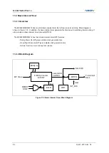
Summary of Contents for MC96FM204
Page 17: ...MC96FM204 FM214 April 7 2016 Ver 1 8 17 4 Package Diagram Figure 4 1 20 Pin SOP Package ...
Page 18: ...MC96FM204 FM214 18 April 7 2016 Ver 1 8 Figure 4 2 20 Pin TSSOP Package ...
Page 19: ...MC96FM204 FM214 April 7 2016 Ver 1 8 19 Figure 4 3 16 Pin SOP Package ...
Page 20: ...MC96FM204 FM214 20 April 7 2016 Ver 1 8 Figure 4 4 16 Pin TSSOP Package ...

