MC96FM204/FM214
April 7, 2016 Ver. 1.8
159
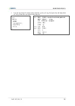
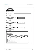
The Byte Write program procedure in user program mode
1. Page buffer clear (FMCR=0x01)
2. Write data to page buffer
3. Set flash sector address register (FSADRH/FSADRM/FSADRL).
4. Set flash identification register (FIDR).
5. Check the UserID for to prevent the invalid work
(Note1).
6. Set flash mode control register (FMCR).
7. Erase verify
Note) 1. Please refer to the chapter
“Protection for Invalid Erase/Write”
2. Data of the address should be
“00H” before writing data to an address
Program Tip
–
byte write
MOV
FMCR,#0x01
;page buffer clear
NOP
;Dummy instruction, This instruction must be needed.
NOP
;Dummy instruction, This instruction must be needed.
NOP
;Dummy instruction, This instruction must be needed.
MOV
A,#5
MOV
DPH,#0x80
;Page Buffer Address is 8000H
MOV
DPL,#0
MOVX @DPTR,A
;Write data to page buffer
MOV
A,#6
MOV
DPH,#0x80
MOV
DPL,#0x05
MOVX @DPTR,A
;Write data to page buffer
MOV
FSADRH,#SAH
;Sector Address High Byte
MOV
FSADRM,#SAM
;Sector Address Middle Byte
MOV
FSADRL,#SAL
;Sector Address Low Byte
MOV
FIDR,#0xA5
;Identification value
MOV
A,#ID_DATA_1
;Check the UserID(written by user)
CJNE A,UserID1,No_WriteErase ;This routine for UserID must be needed.
MOV
A,#ID_DATA_2
CJNE A,UserID2,No_WriteErase
MOV
FMCR,#0x03
;Start flash write mode
NOP
;Dummy instruction, This instruction must be needed.
NOP
;Dummy instruction, This instruction must be needed.
NOP
;Dummy instruction, This instruction must be needed.
LJMP
Write _verify
No_WriteErase:
MOV
FIDR,#00H
MOV
UserID1,#00H
MOV
UserID2,#00H
---
Write_verify:
---
Verify_error:
---
Summary of Contents for MC96FM204
Page 17: ...MC96FM204 FM214 April 7 2016 Ver 1 8 17 4 Package Diagram Figure 4 1 20 Pin SOP Package ...
Page 18: ...MC96FM204 FM214 18 April 7 2016 Ver 1 8 Figure 4 2 20 Pin TSSOP Package ...
Page 19: ...MC96FM204 FM214 April 7 2016 Ver 1 8 19 Figure 4 3 16 Pin SOP Package ...
Page 20: ...MC96FM204 FM214 20 April 7 2016 Ver 1 8 Figure 4 4 16 Pin TSSOP Package ...


