MC96FM204/FM214
April 7, 2016 Ver. 1.8
145
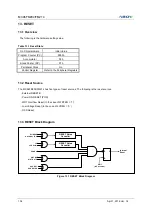
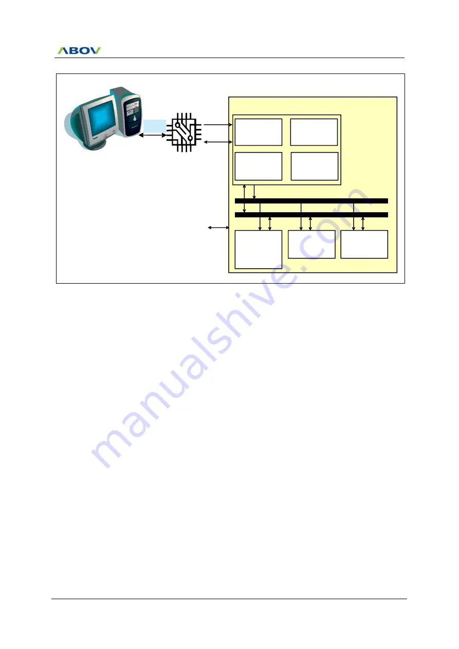
Figure 14.1 Block Diagram of On-Chip Debug System
14.2 Two-Pin External Interface
14.2.1 Basic Transmission Packet
•
10-bit packet transmission using two-pin interface.
•
1-packet consists of 8-bit data, 1-bit parity and 1-bit acknowledge.
•
Parity is even of ‘1’ for 8-bit data in transmitter.
•
Receiver generates acknowledge bit as ‘0’ when transmission for 8-bit data and its parity has no error.
•
When transmitter has no acknowledge
(Acknowledge bit is ‘1’ at tenth clock), error process is executed in
transmitter.
•
When acknowledge error is generated, host PC makes stop condition and transmits command which has error
again.
•
Background debugger command is composed of a bundle of packet.
•
Start condition and stop condition notify the start and the stop of background debugger command respectively.
BDC
Format
converter
USB
CPU
Code memory
-
SRAM
-
Flash
-
EEPROM
Data memory
DBG Register
Peripheral
User I/O
Address bus
Internal data bus
DSDA
DSCL
Target MCU internal circuit
DBG
Control
Summary of Contents for MC96FM204
Page 17: ...MC96FM204 FM214 April 7 2016 Ver 1 8 17 4 Package Diagram Figure 4 1 20 Pin SOP Package ...
Page 18: ...MC96FM204 FM214 18 April 7 2016 Ver 1 8 Figure 4 2 20 Pin TSSOP Package ...
Page 19: ...MC96FM204 FM214 April 7 2016 Ver 1 8 19 Figure 4 3 16 Pin SOP Package ...
Page 20: ...MC96FM204 FM214 20 April 7 2016 Ver 1 8 Figure 4 4 16 Pin TSSOP Package ...


