MC96FM204/FM214
2
April 7, 2016 Ver. 1.8
REVISION HISTORY
VERSION 0.0 (March 15, 2010)
VERSION 1.0 (September 9, 2010)
VERSION 1.1 (November 16, 2010)
Modified Configure option.
Modified Table 13-2 Boot Process Description.
Change ‘150/300uA (Typ/Max)’ to “I
AMP
” in operational amplifier 0/1 characteristics.
VERSION 1.2 (February 14, 2011)
Add Figure 7.9 Recommended Circuit and Layout in Electrical Characteristics.
Add a Note 2 at
‘pin assignment’.
Add a Note at
‘LVRCR register description’.
Add a Note 4 at
‘DSDA and DSCL pins information’.
VERSION 1.3 (July 15, 2011)
Add MC96FM214M/H 16-pin package.
LVRF initial value changed
‘0’ to ‘unknown’.
VERSION 1.4 (November 23, 2011)
Moved more descriptions at T0EN function descriptions.
Add NOTE at
‘LVRVS[3:0] bits description’.
Add
‘Instructions on how to use the input port’ descriptions.
VERSION 1.5 (April 20, 2012)
Change ‘30V/mS (Max)’ to “VDD Voltage Rising Time” in Power-on Reset Electrical characteristics.
Retype a typo at
‘EO Register description’.
VERSION 1.6 (December 5, 2012)
Modified P13IO and P15IO function descriptions.
VERSION 1.7 (April 14, 2015)
Add a note at P0, P1, P2, EIFLAG register description and SFR map.
Change Figure 10.6 and 10.8 in Interrupt.
Add contents of Flash, “Protection for Invalid Erase/Write”.
VERSION 1.8 (April 7, 2016) This book
Add a note in 7.3 A/D Converter Characteristics
Add Flash Data Retention Time in Chapter 7.15 Internal Flash Rom Characteristics
Add a chapter 7.21 Recommended Circuit and Layout with SMPS Power.
Modify the program tips in Chapter 15. Flash Memory.
Add an appendix about “Flash Protection for invalid Erase/Write”
Version 1.8
Published by FAE Team
2016 ABOV Semiconductor Co.,Ltd. All rights reserved.
Additional information of this manual may be served by ABOV Semiconductor offices in Korea or Distributors.
ABOV Semiconductor reserves the right to make changes to any information here in at any time without notice.
The information, diagrams and other data in this manual are correct and reliable; however, ABOV
Semiconductor is in no way responsible for any violations of patents or other rights of the third party
generated by the use of this manual.
Summary of Contents for MC96FM204
Page 17: ...MC96FM204 FM214 April 7 2016 Ver 1 8 17 4 Package Diagram Figure 4 1 20 Pin SOP Package ...
Page 18: ...MC96FM204 FM214 18 April 7 2016 Ver 1 8 Figure 4 2 20 Pin TSSOP Package ...
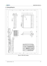
Page 19: ...MC96FM204 FM214 April 7 2016 Ver 1 8 19 Figure 4 3 16 Pin SOP Package ...
Page 20: ...MC96FM204 FM214 20 April 7 2016 Ver 1 8 Figure 4 4 16 Pin TSSOP Package ...


