


Phase-Locked Loop and Clock Dividers
MCF5253 Reference Manual, Rev. 1
Freescale Semiconductor
4-5
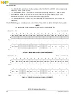
9. If field is “000”, divide by 8
10. Fvcxo min. 200 MHz max. is 400 MHz
11. This bit controls power-down.
12. Faudio is the audio clock. It is LRCK3/AUDIOCLK/GPIO43 when address pin A20/A24 is connected with a pull-up to Vdd, it
is CRIN or CRIN/2 when address pin A20/A24 is connected with a pull-down to GND.
4.2.1
PLL Operation
The input to the PLL is either CRIN, or CRIN divided by two. Selection is done by CRSEL. The PLL
divides this input frequency by a programmable division factor
(PLLDIV)
. In the PLL phase/frequency
detector, this divided clock is compared with the VCXO output clock divided by
(VCXODIV)
. As a result,
Fvcxo = Fin
×
(2
×
VCXODIV) / (PLLDIV).
NOTE
The PLL lock counter is designed for worst case audio input frequency (Fin)
of 33.8688 MHz. This will result in the required 0.5 ms for the PLL to lock.
Other Fin frequencies can be used, however, the resulting lock time will be
slightly longer.
In a second step, this VCXO clock is divided by
(VCXOOUT * CPUDIV)
to create the CPU clock
PSTCLK.
The multiplexers that switch between PLL clock and CRIN is glitch-free, so no system reset is needed
when switching between bypass and PLL modes.
NOTE
It is important that before reprogramming the PLL division factors, users
must switch to PLL bypass mode. After reprogramming, users may
immediately switch back to PLL enabled mode. Switching back is delayed
internally until the PLL is locked.
4.2.2
PLL Lock-In Time
PLL lock time is typically around 10 ms.
4.2.3
PLL Electrical Limits
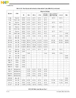
Due to implementation of the block, some limits apply to the PLL block. These limitations are shown in
.
Table 4-5. PLL Electrical Limits
Name
Minimum
Frequency MHz
Maximum
Frequency MHz
Reason
Fvcxo
200
400
PLL limitations
Fcpu
0
140
Maximum operating frequency of device
Fin/PLLDIV
2
8
PLL limitations
Содержание MCF5253
Страница 1: ...Document Number MCF5253RM Rev 1 08 2008 MCF5253 Reference Manual...
Страница 26: ...MCF5253 Reference Manual Rev 1 xxvi Freescale Semiconductor...
Страница 32: ...MCF5253 Reference Manual Rev 1 xxxii Freescale Semiconductor...
Страница 46: ...MCF5253 Introduction MCF5253 Reference Manual Rev 1 1 14 Freescale Semiconductor...
Страница 62: ...Signal Description MCF5253 Reference Manual Rev 1 2 16 Freescale Semiconductor...
Страница 98: ...Instruction Cache MCF5253 Reference Manual Rev 1 5 10 Freescale Semiconductor...
Страница 104: ...Static RAM SRAM MCF5253 Reference Manual Rev 1 6 6 Freescale Semiconductor...
Страница 128: ...Synchronous DRAM Controller Module MCF5253 Reference Manual Rev 1 7 24 Freescale Semiconductor...
Страница 144: ...Bus Operation MCF5253 Reference Manual Rev 1 8 16 Freescale Semiconductor...
Страница 176: ...System Integration Module SIM MCF5253 Reference Manual Rev 1 9 32 Freescale Semiconductor...
Страница 198: ...Analog to Digital Converter ADC MCF5253 Reference Manual Rev 1 12 6 Freescale Semiconductor...
Страница 246: ...DMA Controller MCF5253 Reference Manual Rev 1 14 18 Freescale Semiconductor...
Страница 282: ...UART Modules MCF5253 Reference Manual Rev 1 15 36 Freescale Semiconductor...
Страница 298: ...Queued Serial Peripheral Interface QSPI Module MCF5253 Reference Manual Rev 1 16 16 Freescale Semiconductor...
Страница 344: ...Audio Interface Module AIM MCF5253 Reference Manual Rev 1 17 46 Freescale Semiconductor...
Страница 362: ...I2 C Modules MCF5253 Reference Manual Rev 1 18 18 Freescale Semiconductor...
Страница 370: ...Boot ROM MCF5253 Reference Manual Rev 1 19 8 Freescale Semiconductor...


