

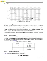


System Integration Module (SIM)
MCF5253 Reference Manual, Rev. 1
9-6
Freescale Semiconductor
9.3.2
Device ID Register
The DeviceID register is a read only register that allows the software to determine what hardware it is
running on. The register contains the part number in the upper 24 bits, the mask revision number in the
lower 8 bits, and is read as 0x005251rr, where
rr
is the revision number.
This register allows developers the flexibility to write code to run on more than one device. The revision
number allows developers to distinguish between different mask versions that may have minor changes or
bug fixes. For example, developers may want to distribute a single code image or library for use on
different revisions of the silicon.
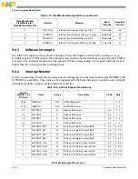
9.4
Interrupt Interface Registers
For legacy reasons, there are two interrupt controllers on the MCF5253. This section provides the
programming of the two interrupt controller registers and their register descriptions.
The primary interrupt controller is centralized, and services the following:
•
Software Watchdog Timer (SWT)
•
Timer modules
•
I
2
C0 module
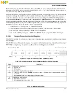
7–1
LS
If interrupts in both the “primary” and the “secondary” interrupt controllers have the same interrupt level pending
then bits LS[7:1] determine which interrupt controller gets priority.
If the bit is cleared, the primary interrupt controller gets priority. If the bit is set, the secondary interrupt controller
gets priority.
There are 7 LSn bits, one for each interrupt level.
0
V
The Valid bit defines if the CPU can access the MBAR2 mapped peripherals.
0 MBAR2 address space not visible by CPU
1 MBAR2 address space visible by CPU
Address MBAR2 + 0xAC
Access: User read
31
30
29
28
27
26
25
24
23
22
21
20
19
18
17
16
R
Part Number
W
Reset
0
0
0
0
0
0
0
0
0
1
0
1
0
0
1
0
15
14
13
12
11
10
9
8
7
6
5
4
3
2
1
0
R
Part Number
Mask Revision
W
Reset
0
1
0
1
0
0
0
1
–
–
–
–
–
–
–
0
Figure 9-3. DeviceID Register (DeviceID)
Table 9-4. Second Module Base Address Register (MBAR2)Field Descriptions (continued)
Field
Description
Содержание MCF5253
Страница 1: ...Document Number MCF5253RM Rev 1 08 2008 MCF5253 Reference Manual...
Страница 26: ...MCF5253 Reference Manual Rev 1 xxvi Freescale Semiconductor...
Страница 32: ...MCF5253 Reference Manual Rev 1 xxxii Freescale Semiconductor...
Страница 46: ...MCF5253 Introduction MCF5253 Reference Manual Rev 1 1 14 Freescale Semiconductor...
Страница 62: ...Signal Description MCF5253 Reference Manual Rev 1 2 16 Freescale Semiconductor...
Страница 98: ...Instruction Cache MCF5253 Reference Manual Rev 1 5 10 Freescale Semiconductor...
Страница 104: ...Static RAM SRAM MCF5253 Reference Manual Rev 1 6 6 Freescale Semiconductor...
Страница 128: ...Synchronous DRAM Controller Module MCF5253 Reference Manual Rev 1 7 24 Freescale Semiconductor...
Страница 144: ...Bus Operation MCF5253 Reference Manual Rev 1 8 16 Freescale Semiconductor...
Страница 176: ...System Integration Module SIM MCF5253 Reference Manual Rev 1 9 32 Freescale Semiconductor...
Страница 198: ...Analog to Digital Converter ADC MCF5253 Reference Manual Rev 1 12 6 Freescale Semiconductor...
Страница 246: ...DMA Controller MCF5253 Reference Manual Rev 1 14 18 Freescale Semiconductor...
Страница 282: ...UART Modules MCF5253 Reference Manual Rev 1 15 36 Freescale Semiconductor...
Страница 298: ...Queued Serial Peripheral Interface QSPI Module MCF5253 Reference Manual Rev 1 16 16 Freescale Semiconductor...
Страница 344: ...Audio Interface Module AIM MCF5253 Reference Manual Rev 1 17 46 Freescale Semiconductor...
Страница 362: ...I2 C Modules MCF5253 Reference Manual Rev 1 18 18 Freescale Semiconductor...
Страница 370: ...Boot ROM MCF5253 Reference Manual Rev 1 19 8 Freescale Semiconductor...


