XRT86VL38
PRELIMINARY
xr
OCTAL T1/E1/J1 FRAMER/LIU COMBO
REV. P1.0.6
63
3.3.1
The PowerPC 403 Read-Cycle
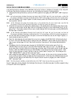
If the Microprocessor Interface (of the XRT86VL38 device) has been configured to operate in the PowerPC
403 Mode, then the Microprocessor should do all of the following to perfrom a read operation:
1.
As the Microprocessor executes all of the following steps, it should designate this particular bus cycle as a
READ Operation by making sure that the WR*/R/W* (R/W*) input pin is held at a logic "high".
2.
2. Place the address of the "target" register or buffer location (within the XRT86VL38 device) on the
Address Bus input pin, A[14:0].
N
OTE
: As the Microprocessor places this address value, on the Address Bus, the user should make sure that the
Microprocessor respects the "Address to Rising edge of PCLK Set-up time" requirements.)
PCLK
Y25
V22
I
Microprocessor Interface Clock Input:
This clock input signal is only used if the Microprocessor Interface has been con-
figured to operate in Synchronous Mode (i.e., Power PC 403 Mode). If the
Microprocessor Interface is configured to operate in Power PC mode, then it will
use this clock signal to do the following.·
1) To sample the CS*, WR*/R/W*, A[14:0], D[7:0], RD*/DS* and DBEN input
pins,
2) To update the state of the D[7:0] and the RDY/DTACK output signals.
N
OTE
: The Microprocessor Interface can work with PCLK frequencies ranging
up to 33MHz.
WR*/R/
W*
M23
L20
I
Read/Write Operation Identification Input - R/W*
If the Microprocessor Interface is configured to operate in the Power PC 403
Mode, then this input pin will function as the "Read/Write Operation Identification
Input" pin. Anytime the Microprocessor Interface samples this input signal at a
logic low (while also sampling the CS* input pin "low") upon the rising edge of
PCLK, then the Microprocessor Interface will (upon the very same rising edge of
PCLK) latch the contents of the Address Bus (A[14:0]) into the Microprocessor
Interface circuitry, in preparation for this forthcoming READ operation.
At some point (later in this READ operation) the Microprocessor will also assert
the DBEN*/OE* input pin, and the Microprocessor Interface will then place the
contents of the "target" register (or address location within the XRT86VL38
device) upon the Bi-Directional Data Bus pins (D[7:0]), where it can be read by
the Microprocessor.Anytime the Microprocessor Interface samples this input sig-
nal at a logic high (while also sampling the CS* input pin a logic "low") upon the
rising edge of PCLK, then the Microprocessor Interface will (upon the very same
rising edge of PCLK) latch the contents of the Address Bus (A[14:0]) into the
Microprocessor Interface circuitry, in preparation for the forthcoming WRITE
operation.
At some point (later in this WRITE operation) the Microprocessor will also assert
the RD*/DS*/WE* input pin, and the Microprocessor Interface will then latch the
contents of the Bi-Directional Data Bus (D[7:0]) into the contents of the "target"
register or buffer location (within the XRT86VL38 device).
DBEN*
V23
U22
I
Data Bus Enable Input:
Data Bus Enable Input: For PowerPC Mode operation, the user should tie this
pin to the OE* output (from the MPC860/8260 Microprocessor, or similar
pin).This input pin will be sampled upon the rising edge of PCLK.
BLAST
P23
M17
I
NONE - Tie this pin to GND
T
ABLE
8: T
HE
R
OLES
OF
V
ARIOUS
M
ICROPROCESSOR
I
NTERFACE
P
INS
,
WHEN
CONFIGURED
TO
OPERATE
IN
THE
P
OWER
PC M
ODE
P
IN
N
AME
420 P
KG
B
ALL
#
484 P
KG
B
ALL
#
T
YPE
D
ESCRIPTION


