427
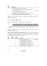
Bits 3 to 0: These bits operate as in normal serial communication. For details see section 12.2.7,
Serial Status Register (SSR). The setting conditions for transmit end (TEND), however, are
modified as follows.
Bit 2
TEND
Description
0
Transmission is in progress
[Clearing condition]
Software reads TDRE while it is set to 1, then writes 0 in the TDRE flag.
1
End of transmission
[Setting conditions]
(Initial value)
•
The chip is reset or enters standby mode.
•
The TE bit and FER/ERS bit are both cleared to 0 in SCR.
•
TDRE is 1 and FER/ERS is 0 at a time 2.5 etu after the last bit of a 1-byte serial
character is transmitted (normal transmission).
Note:
An etu (elementary time unit) is the time needed to transmit one bit.
13.2.3
Serial Mode Register (SMR)
The function of SMR bit 7 is modified in smart card interface mode. This change also causes a
modification to the function of bits 1 and 0 in the serial control register (SCR).
7
GM
0
R/W
6
CHR
0
R/W
5
PE
0
R/W
4
O/E
0
R/W
3
STOP
0
R/W
0
CKS0
0
R/W
2
MP
0
R/W
1
CKS1
0
R/W
Bit
Initial value
Read/Write
Bit 7—GSM Mode (GM): With the normal smart card interface, this bit is cleared to 0. Setting
this bit to 1 selects GSM mode, an additional mode for controlling the timing for setting the
TEND flag that indicates completion of transmission, and the type of clock output used. The
details of the additional clock output control mode are specified by the CKE1 and CKE0 bits in
the serial control register (SCR).
Summary of Contents for H8/3060
Page 10: ......
Page 16: ......
Page 114: ...66 ...
Page 132: ...84 ...
Page 144: ...96 ...
Page 170: ...122 ...
Page 212: ...164 ...
Page 268: ...220 ...
Page 332: ...284 ...
Page 396: ...348 ...
Page 494: ...446 ...
Page 698: ...650 ...
Page 748: ...700 H8 3064F ZTAT B mask version Ports 1 2 5 LED 600 Ω Figure 22 8 Sample LED Circuit ...
Page 777: ...729 H8 3062F ZTAT B mask version Ports 1 2 5 LED 600 Ω Figure 22 14 Sample LED Circuit ...
Page 810: ...762 ...
Page 994: ...946 ...


