333
10.2.7
Next Data Enable Register A (NDERA)
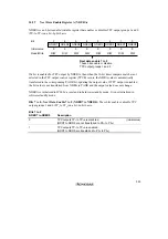
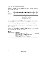
NDERA is an 8-bit readable/writable register that enables or disables TPC output groups 1 and 0
(TP
7
to TP
0
) on a bit-by-bit basis.
Bit
Initial value
Read/Write
0
NDER0
0
R/W
1
NDER1
0
R/W
2
NDER2
0
R/W
3
NDER3
0
R/W
4
NDER4
0
R/W
5
NDER5
0
R/W
6
NDER6
0
R/W
7
NDER7
0
R/W
Next data enable 7 to 0
These bits enable or disable
TPC output groups 1 and 0
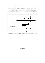
If a bit is enabled for TPC output by NDERA, then when the 16-bit timer compare match event
selected in the TPC output control register (TPCR) occurs, the NDRA value is automatically
transferred to the corresponding PADR bit, updating the output value. If TPC output is disabled,
the bit value is not transferred from NDRA to PADR and the output value does not change.
NDERA is initialized to H'00 by a reset and in hardware standby mode. It is not initialized in
software standby mode.
Bits 7 to 0—Next Data Enable 7 to 0 (NDER7 to NDER0): These bits enable or disable TPC
output groups 1 and 0 (TP
7
to TP
0
) on a bit-by-bit basis.
Bits 7 to 0
NDER7 to NDER0
Description
0
TPC outputs TP
7
to TP
0
are disabled
(NDR7 to NDR0 are not transferred to PA
7
to PA
0
)
(Initial value)
1
TPC outputs TP
7
to TP
0
are enabled
(NDR7 to NDR0 are transferred to PA
7
to PA
0
)
Summary of Contents for H8/3060
Page 10: ......
Page 16: ......
Page 114: ...66 ...
Page 132: ...84 ...
Page 144: ...96 ...
Page 170: ...122 ...
Page 212: ...164 ...
Page 268: ...220 ...
Page 332: ...284 ...
Page 396: ...348 ...
Page 494: ...446 ...
Page 698: ...650 ...
Page 748: ...700 H8 3064F ZTAT B mask version Ports 1 2 5 LED 600 Ω Figure 22 8 Sample LED Circuit ...
Page 777: ...729 H8 3062F ZTAT B mask version Ports 1 2 5 LED 600 Ω Figure 22 14 Sample LED Circuit ...
Page 810: ...762 ...
Page 994: ...946 ...

