428
Bit 7
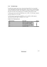
GM
Description
0
Normal smart card interface mode operation
•
The TEND flag is set 12.5 etu after the beginning of the start bit.
•
Clock output on/off control only.
(Initial value)
1
GSM mode smart card interface mode operation
•
The TEND flag is set 11.0 etu after the beginning of the start bit.
•
Clock output on/off and fixed-high/fixed-low control.
Bits 6 to 0: These bits operate as in normal serial communication. For details see section 12.2.5,
Serial Mode Register (SMR).
13.2.4
Serial Control Register (SCR)
The function of SCR bits 1 and 0 is modified in smart card interface mode.
7
TIE
0
R/W
6
RIE
0
R/W
5
TE
0
R/W
4
RE
0
R/W
3
MPIE
0
R/W
0
CKE0
0
R/W
2
TEIE
0
R/W
1
CKE1
0
R/W
Bit
Initial value
Read/Write
Bits 7 to 2: These bits operate as in normal serial communication. For details see section 12.2.6,
Serial Control Register (SCR).
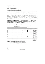
Bits 1 and 0—Clock Enable 1 and 0 (CKE1, CKE0): These bits select the SCI clock source and
enable or disable clock output from the SCK pin. In smart card interface mode, it is possible to
specify a fixed high level or fixed low level for the clock output, in addition to the usual switching
between enabling and disabling of the clock output.
Bit 7
GM
Bit 1
CKE1
Bit 0
CKE0
Description
0
0
0
Internal clock/SCK pin is I/O port
(Initial value)
1
Internal clock/SCK pin is clock output
1
0
Internal clock/SCK pin is fixed at low output
1
Internal clock/SCK pin is clock output
1
0
Internal clock/SCK pin is fixed at high output
1
Internal clock/SCK pin is clock output
Summary of Contents for H8/3060
Page 10: ......
Page 16: ......
Page 114: ...66 ...
Page 132: ...84 ...
Page 144: ...96 ...
Page 170: ...122 ...
Page 212: ...164 ...
Page 268: ...220 ...
Page 332: ...284 ...
Page 396: ...348 ...
Page 494: ...446 ...
Page 698: ...650 ...
Page 748: ...700 H8 3064F ZTAT B mask version Ports 1 2 5 LED 600 Ω Figure 22 8 Sample LED Circuit ...
Page 777: ...729 H8 3062F ZTAT B mask version Ports 1 2 5 LED 600 Ω Figure 22 14 Sample LED Circuit ...
Page 810: ...762 ...
Page 994: ...946 ...


