860
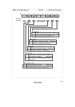
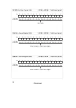
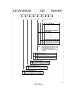
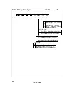
GRA1 H/L—General Register A1 H/L
H’FFF74, H’FFF75
16-bit timer channel 1
Bit
Initial value
Read/Write
1
R/W
1
R/W
1
R/W
1
R/W
1
R/W
1
R/W
1
R/W
1
R/W
15
14
13
12
11
10
9
8
7
6
5
4
3
2
1
0
1
R/W
1
R/W
1
R/W
1
R/W
1
R/W
1
R/W
1
R/W
1
R/W
*Bit functions are the same as for 16-bit timer channel 0.
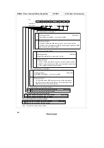
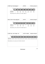
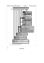
GRB1 H/L—General Register B1 H/L
H’FFF76, H’FFF77
16-bit timer channel 1
Bit
Initial value
Read/Write
1
R/W
1
R/W
1
R/W
1
R/W
1
R/W
1
R/W
1
R/W
1
R/W
15
14
13
12
11
10
9
8
7
6
5
4
3
2
1
0
1
R/W
1
R/W
1
R/W
1
R/W
1
R/W
1
R/W
1
R/W
1
R/W
*Bit functions are the same as for 16-bit timer channel 0.
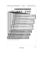
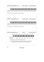
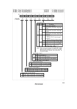
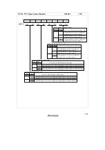
16TCR2 Timer Control Register 2
H’FFF78
16-bit timer channel 2
7
—
1
—
Bit
Initial value
Read/Write
6
CCLR1
0
R/W
5
CCLR0
0
R/W
4
CKEG1
0
R/W
3
CKEG0
0
R/W
2
TPSC2
0
R/W
1
TPSC1
0
R/W
0
TPSC0
0
R/W
*Bit functions are the same as for 16-bit timer channel 0.
Note : When phase counting mode is selected in channel 2, the settings of bits
CKEG1 and CKEG0 and TPSC2 to TPSC0 in 16TCR2 are ignored.
Summary of Contents for H8/3060
Page 10: ......
Page 16: ......
Page 114: ...66 ...
Page 132: ...84 ...
Page 144: ...96 ...
Page 170: ...122 ...
Page 212: ...164 ...
Page 268: ...220 ...
Page 332: ...284 ...
Page 396: ...348 ...
Page 494: ...446 ...
Page 698: ...650 ...
Page 748: ...700 H8 3064F ZTAT B mask version Ports 1 2 5 LED 600 Ω Figure 22 8 Sample LED Circuit ...
Page 777: ...729 H8 3062F ZTAT B mask version Ports 1 2 5 LED 600 Ω Figure 22 14 Sample LED Circuit ...
Page 810: ...762 ...
Page 994: ...946 ...


