533
Note:
Bits 7 to 4 in this register are read-only. These bits must not be set to 1. If bits 7 to 4 are
set when an EBR1/EBR2 bit is set, EBR1/EBR2 will be initialized to H'00.
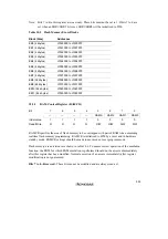
Table 18.5
Flash Memory Erase Blocks
Block (Size)
Addresses
EB0 (4 kbytes)
H'000000 to H'000FFF
EB1 (4 kbytes)
H'001000 to H'001FFF
EB2 (4 kbytes)
H'002000 to H'002FFF
EB3 (4 kbytes)
H'003000 to H'003FFF
EB4 (4 kbytes)
H'004000 to H'004FFF
EB5 (4 kbytes)
H'005000 to H'005FFF
EB6 (4 kbytes)
H'006000 to H'006FFF
EB7 (4 kbytes)
H'007000 to H'007FFF
EB8 (32 kbytes)
H'008000 to H'00FFFF
EB9 (64 kbytes)
H'010000 to H'01FFFF
EB10 (64 kbytes)
H'020000 to H'02FFFF
EB11 (64 kbytes)
H'030000 to H'03FFFF
18.3.5
RAM Control Register (RAMCR)
Bit
7
6
5
4
3
2
1
0
—
—
—
—
RAMS
RAM2
RAM1
RAM0
Initial value
1
1
1
1
0
0
0
0
Read/Write
R
R
R
R
R/W
R/W
R/W
R/W
RAMCR specifies the area of flash memory to be overlapped with part of RAM when emulating
realtime flash memory programming. RAMCR is initialized to H'00 by a reset and in hardware
standby mode. RAMCR settings should be made in user mode or user program mode.
Flash memory area divisions are shown in table 18.6. To ensure correct operation of the emulation
function, the ROM for which RAM emulation is performed should not be accessed immediately
after this register has been modified. Normal execution of an access immediately after register
modification is not guaranteed.
Bits 7 to 4—Reserved: These bits cannot be modified and are always read as 1.
Summary of Contents for H8/3060
Page 10: ......
Page 16: ......
Page 114: ...66 ...
Page 132: ...84 ...
Page 144: ...96 ...
Page 170: ...122 ...
Page 212: ...164 ...
Page 268: ...220 ...
Page 332: ...284 ...
Page 396: ...348 ...
Page 494: ...446 ...
Page 698: ...650 ...
Page 748: ...700 H8 3064F ZTAT B mask version Ports 1 2 5 LED 600 Ω Figure 22 8 Sample LED Circuit ...
Page 777: ...729 H8 3062F ZTAT B mask version Ports 1 2 5 LED 600 Ω Figure 22 14 Sample LED Circuit ...
Page 810: ...762 ...
Page 994: ...946 ...


