419
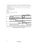
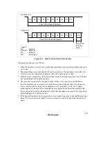
Switching from SCK Pin Function to Port Pin Function:
•
Problem in Operation: When switching the SCK pin function to the output port function (high-
level output) by making the following settings while DDR = 1, DR = 1, C/
A
= 1, CKE1 = 0,
CKE0 = 0, and TE = 1 (synchronous mode), low-level output occurs for one half-cycle.
1. End of serial data transmission
2. TE bit = 0
3. C/
A
bit = 0 ... switchover to port output
4. Occurrence of low-level output (see figure 12.23)
SCK/port
Data
TE
C/A
CKE1
CKE0
Bit 7
Bit 6
1. End of transmission
4. Low-level output
3.C/A= 0
2.TE= 0
Half-cycle low-level output
Figure 12.23 Operation when Switching from SCK Pin Function to Port Pin Function
Summary of Contents for H8/3060
Page 10: ......
Page 16: ......
Page 114: ...66 ...
Page 132: ...84 ...
Page 144: ...96 ...
Page 170: ...122 ...
Page 212: ...164 ...
Page 268: ...220 ...
Page 332: ...284 ...
Page 396: ...348 ...
Page 494: ...446 ...
Page 698: ...650 ...
Page 748: ...700 H8 3064F ZTAT B mask version Ports 1 2 5 LED 600 Ω Figure 22 8 Sample LED Circuit ...
Page 777: ...729 H8 3062F ZTAT B mask version Ports 1 2 5 LED 600 Ω Figure 22 14 Sample LED Circuit ...
Page 810: ...762 ...
Page 994: ...946 ...


