567
•
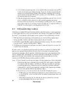
Apply FWE when the V
CC
voltage has stabilized within its rated voltage range.
If FWE is applied when the MCU’s V
CC
power supply is not within its rated voltage range,
MCU operation will be unstable and flash memory may be erroneously programmed or
erased.
•
Apply FWE when oscillation has stabilized (after the elapse of the oscillation settling
time).
When V
CC
power is turned on, hold the
RES
pin low for the duration of the oscillation
settling time before applying FWE. Do not apply FWE when oscillation has stopped or is
unstable.
•
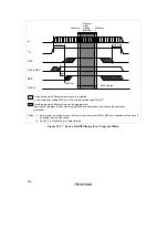
In boot mode, apply and disconnect FWE during a reset.
In a transition to boot mode, FWE = 1 input and MD
2
to MD
0
setting should be performed
while the
RES
input is low. FWE and MD
2
to MD
0
pin input must satisfy the mode
programming setup time (t
MDS
) with respect to the reset release timing. When making a
transition from boot mode to another mode, also, a mode programming setup time is
necessary with respect to the reset release timing.
In a reset during operation, the
RES
pin must be held low for a minimum of 20 system
clock cycles.
•
In user program mode, FWE can be switched between high and low level regardless of
RES
input.
FWE input can also be switched during execution of a program in flash memory.
•
Do not apply FWE if program runaway has occurred.
During FWE application, the program execution state must be monitored using the
watchdog timer or some other means.
•
Disconnect FWE only when the SWE, ESU, PSU, EV, PV, E, and P bits in FLMCR1 are
cleared.
Make sure that the SWE, ESU, PSU, EV, PV, E, and P bits are not set by mistake when
applying or disconnecting FWE.
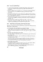
4. Do not apply a constant high level to the FWE pin.
T prevent erroneous programming or erasing due to program runaway, etc., apply a high level
to the FWE pin only when programming or erasing flash memory (including execution of flash
memory emulation using RAM). A system configuration in which a high level is constantly
applied to the FWE pin should be avoided. Also, while a high level is applied to the FWE pin,
the watchdog timer should be activated to prevent overprogramming or overerasing due to
program runaway, etc.
5. Use the recommended algorithm when programming and erasing flash memory.
The recommended algorithm enables programming and erasing to be carried out without
subjecting the device to voltage stress or sacrificing program data reliability. When setting the
PSU or ESU bit in FLMCR1, the watchdog timer should be set beforehand as a precaution
against program runaway, etc.
Summary of Contents for H8/3060
Page 10: ......
Page 16: ......
Page 114: ...66 ...
Page 132: ...84 ...
Page 144: ...96 ...
Page 170: ...122 ...
Page 212: ...164 ...
Page 268: ...220 ...
Page 332: ...284 ...
Page 396: ...348 ...
Page 494: ...446 ...
Page 698: ...650 ...
Page 748: ...700 H8 3064F ZTAT B mask version Ports 1 2 5 LED 600 Ω Figure 22 8 Sample LED Circuit ...
Page 777: ...729 H8 3062F ZTAT B mask version Ports 1 2 5 LED 600 Ω Figure 22 14 Sample LED Circuit ...
Page 810: ...762 ...
Page 994: ...946 ...


