527
18.2.2
Pin Configuration
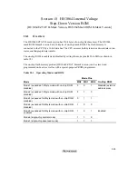
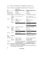
The flash memory is controlled by means of the pins shown in table 18.3.
Table 18.3
Flash Memory Pins
Pin Name
Abbreviation
I/O
Function
Reset
RES
Input
Reset
Flash write enable
FWE
Input
Flash program/erase protection by hardware
Mode 2
MD
2
Input
Sets H8/3064F-ZTAT B-mask version
operating mode
Mode 1
MD
1
Input
Sets H8/3064F-ZTAT B-mask version
operating mode
Mode 0
MD
0
Input
Sets H8/3064F-ZTAT B-mask version
operating mode
Transmit data
TxD
1
Output
Serial transmit data output
Receive data
RxD
1
Input
Serial receive data input
18.2.3
Register Configuration
The registers used to control the on-chip flash memory when enabled are shown in table 18.4.
Table 18.4
Flash Memory Registers
Register Name
Abbreviation
R/W
Initial Value
Address
*
1
Flash memory control register 1
FLMCR1
R/W
H'00
*
2
H'EE030
Flash memory control register 2
FLMCR2
R
H'00
H'EE031
Erase block register 1
EBR1
R/W
H'00
H'EE032
Erase block register 2
EBR2
R/W
H'00
H'EE033
RAM control register
RAMCR
R/W
H'F0
H'EE077
Notes: FLMCR1, FLMCR2, EBR1, EBR2, and RAMCR are 8-bit registers,
and should be
accessed by byte access . These registers are used only in the versions with on-chip flash
memory, and are not provided in the versions with on-chip mask ROM. Reading the
corresponding addresses in a mask ROM version will always return 1s, and writes to these
addresses are invalid.
*
1 Lower 20 bits of address in advanced mode
*
2 When a high level is input to the FWE pin, the initial value is H'80.
Summary of Contents for H8/3060
Page 10: ......
Page 16: ......
Page 114: ...66 ...
Page 132: ...84 ...
Page 144: ...96 ...
Page 170: ...122 ...
Page 212: ...164 ...
Page 268: ...220 ...
Page 332: ...284 ...
Page 396: ...348 ...
Page 494: ...446 ...
Page 698: ...650 ...
Page 748: ...700 H8 3064F ZTAT B mask version Ports 1 2 5 LED 600 Ω Figure 22 8 Sample LED Circuit ...
Page 777: ...729 H8 3062F ZTAT B mask version Ports 1 2 5 LED 600 Ω Figure 22 14 Sample LED Circuit ...
Page 810: ...762 ...
Page 994: ...946 ...


