355
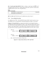
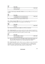
Bit 6—Reset Output Enable (RSTOE): Enables or disables external output at the
RESO
pin of
the reset signal generated if TCNT overflows during watchdog timer operation. Note that there is
no
RESO
pin in the versions with on-chip flash memory.
Bit 6
RSTOE
Description
0
Reset signal is not output externally
(Initial value)
1
Reset signal is output externally
Bits 5 to 0—Reserved: These bits cannot be modified and are always read as 1.
11.2.4
Notes on Register Rewriting
The watchdog timer’s TCNT, TCSR, and RSTCSR registers differ from other registers in being
more difficult to write. The procedures for writing and reading these registers are given below.
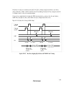
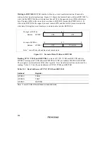
Writing to TCNT and TCSR: These registers must be written by a word transfer instruction.
They cannot be written by byte instructions. Figure 11.2 shows the format of data written to TCNT
and TCSR. TCNT and TCSR both have the same write address. The write data must be contained
in the lower byte of the written word. The upper byte must contain H'5A (password for TCNT) or
H'A5 (password for TCSR). This transfers the write data from the lower byte to TCNT or TCSR.
15
8 7
0
H'5A
Write data
Address
H'FFF8C
*
15
8 7
0
H'A5
Write data
Address
H'FFF8C
*
TCNT write
TCSR write
Note:
*
Lower 20 bits of the address in advanced mode
Figure 11.2 Format of Data Written to TCNT and TCSR
Summary of Contents for H8/3060
Page 10: ......
Page 16: ......
Page 114: ...66 ...
Page 132: ...84 ...
Page 144: ...96 ...
Page 170: ...122 ...
Page 212: ...164 ...
Page 268: ...220 ...
Page 332: ...284 ...
Page 396: ...348 ...
Page 494: ...446 ...
Page 698: ...650 ...
Page 748: ...700 H8 3064F ZTAT B mask version Ports 1 2 5 LED 600 Ω Figure 22 8 Sample LED Circuit ...
Page 777: ...729 H8 3062F ZTAT B mask version Ports 1 2 5 LED 600 Ω Figure 22 14 Sample LED Circuit ...
Page 810: ...762 ...
Page 994: ...946 ...


