350
11.1.2
Block Diagram
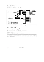
Figure 11.1 shows a block diagram of the WDT.
φ
/2
φ
/32
φ
/64
φ
/128
φ
/256
φ
/512
φ
/2048
φ
/4096
TCNT
TCSR
RSTCSR
Reset control
Interrupt signal
Reset
(internal, external)
(interval timer)
Interrupt
control
Overflow
Clock
Clock
selector
Read/
write
control
Internal
data bus
Internal clock sources
Legend:
TCNT
:
TCSR
:
RSTCSR :
Timer counter
Timer control/status register
Reset control/status register
Figure 11.1 WDT Block Diagram
11.1.3
Pin Configuration
Table 11.1 describes the WDT output pin*.
Note: * Not present in the versions with on-chip flash memory.
Table 11.1
WDT Pin
Name
Abbreviation
I/O
Function
Reset output
RESO
Output
*
External output of the watchdog timer reset signal
Note:
*
Open-drain output
Summary of Contents for H8/3060
Page 10: ......
Page 16: ......
Page 114: ...66 ...
Page 132: ...84 ...
Page 144: ...96 ...
Page 170: ...122 ...
Page 212: ...164 ...
Page 268: ...220 ...
Page 332: ...284 ...
Page 396: ...348 ...
Page 494: ...446 ...
Page 698: ...650 ...
Page 748: ...700 H8 3064F ZTAT B mask version Ports 1 2 5 LED 600 Ω Figure 22 8 Sample LED Circuit ...
Page 777: ...729 H8 3062F ZTAT B mask version Ports 1 2 5 LED 600 Ω Figure 22 14 Sample LED Circuit ...
Page 810: ...762 ...
Page 994: ...946 ...

