680
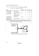
Table 22.13 Permissible Output Currents
Conditions: V
CC
= 3.0 V to 5.5 V, AV
CC
= 3.0 V to 5.5 V, V
REF
= 3.0 V to AV
CC
,
V
SS
= AV
SS
= 0 V, T
a
= –20°C to +75°C (regular specifications),
T
a
= –40°C to +85°C (wide-range specifications)
Item
Symbol
Min
Typ
Max
Unit
Permissible output
low current (per pin)
Ports 1, 2, and 5
Other output pins
I
OL
—
—
—
—
10
2.0
mA
mA
Permissible output
low current (total)
Sum of 20 pins in ports 1,
2, and 5
Σ
I
OL
—
—
80
mA
Total of all output pins,
including the above
—
—
120
mA
Permissible output
high current (per pin)
All output pins
|–I
OH
|
—
—
2.0
mA
Permissible output
high current (total)
Total of all output pins
|
–
Σ
I
OH
|
—
—
40
mA
Notes: 1. To protect chip reliability, do not exceed the output current values in table 22.13.
2. When directly driving a darlington pair or LED, always insert a current-limiting resistor in
the output line, as shown in figures 22.4 and 22.5.
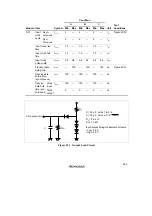
H8/3062F-ZTAT or
H8/3062F-ZTAT
R-mask version
Port
2 k
Ω
Darlington pair
Figure 22.4 Darlington Pair Drive Circuit (Example)
Summary of Contents for H8/3060
Page 10: ......
Page 16: ......
Page 114: ...66 ...
Page 132: ...84 ...
Page 144: ...96 ...
Page 170: ...122 ...
Page 212: ...164 ...
Page 268: ...220 ...
Page 332: ...284 ...
Page 396: ...348 ...
Page 494: ...446 ...
Page 698: ...650 ...
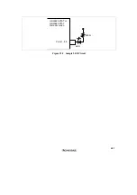
Page 748: ...700 H8 3064F ZTAT B mask version Ports 1 2 5 LED 600 Ω Figure 22 8 Sample LED Circuit ...
Page 777: ...729 H8 3062F ZTAT B mask version Ports 1 2 5 LED 600 Ω Figure 22 14 Sample LED Circuit ...
Page 810: ...762 ...
Page 994: ...946 ...


