


10 Process Data Objects (PDO)
48
YASKAWA ELECTRIC
SIEP C730600 64A 1000-Series Option SI-ES3 Technical Manual
Receive PDOs (RxPDO)
The Receive PDOs have a default mapping according to
Table 16
. The end user can re-map Receive PDOs by writing to
the map objects 0x1600-1628. Refer to
Communication Profile Objects (DSP 301) on page 26
.
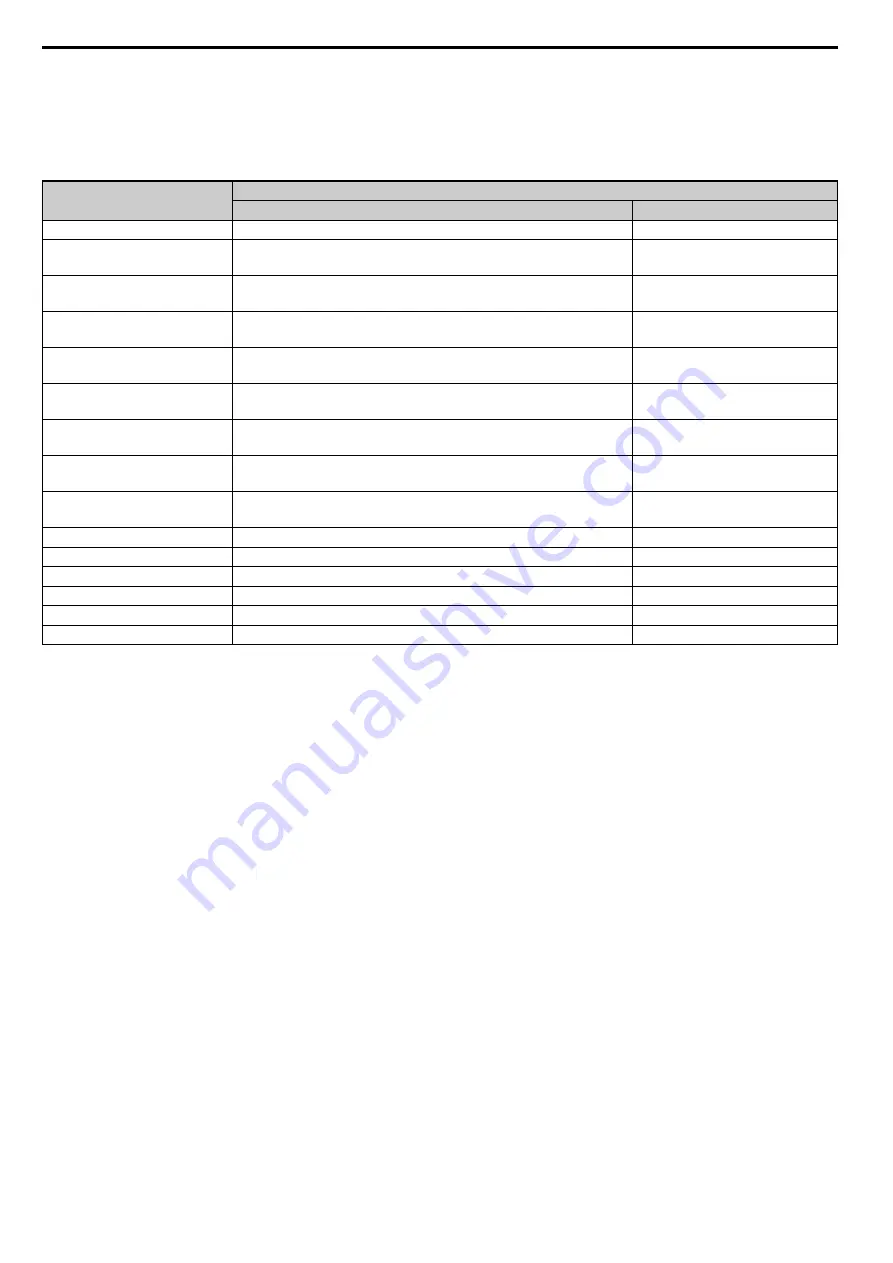
Table 16 Receive PDO
RxPDO Mapped Drive Registers Above 0x0100 Range
Drive registers above 0x0100 cannot be configured as process data exchanged on each I/F scan cycle. To be able to
RxPDO map those objects on EtherCAT, a “slow” IO channel must be realized inside the option system firmware. This
slow IO channel uses the overlaid MEMOBUS/Modbus channel in I/F to write the drive registers required.
When the RxPDO mapping is performed on any drive register and the address is larger than 0x0100, it will be added to
the slow IO control set.
ENTER command management for slow IO channel control sets:
• New value only written against drive if it changes from the previously written value.
• If a value update is detected, the write will be scheduled directly after the RxPDO EtherCAT process data cycle is
complete.
• If the written value via MEMOBUS/Modbus fails, i.e. parameter cannot be written when the drive is running, a new
retry will be triggered after 8 ms.
• If a RAM ENTER command is required for the written value to be used by the drive, the ENTER command will be
written when the last register that should be updated in an slow IO data scan set update is triggered.
• Mapped drive registers: A: 0x0200, B: 0x0201, C: 0x0203
• All three registers change at the same time: RAM ENTER command executed with C.
• Only register 0x0200 changes: RAM ENTER command executed with A.
PDO Number
Receive PDO Mapping
Mapped Objects (Hex)
Index (Hex)
1
Sub-index 1: 0x6040#0, 2-bytes (DSP402 controlword)
0x1600
2
Sub-index 1: 0x6040#0, 2-bytes (DSP402 controlword)
Sub-index 2: 0x6060#0, 1-bytes (DSP402 modes of operation)
0x1601
6
Sub-index 1: 0x6040#0, 2-bytes (DSP402 controlword)
Sub-index 2: 0x6042#0, 2-bytes (vl target velocity)
0x1605
7
Sub-index 1: 0x6040#0, 2-bytes (DSP402 controlword)
Sub-index 2: 0x60FE#1, 4-bytes (Physical digital outputs)
0x1606
8
Sub-index 1: 0x6040#0, 2-bytes (DSP402 controlword)
Sub-index 2: 0x6060#0, 1-bytes (DSP402 modes of operation)
0x1607
21
Sub-index 1: 0x6048#1, 4-bytes (vl accel delta speed)
Sub-index 2: 0x6048#2, 2-bytes (vl accel delta time)
0x1614
22
Sub-index 1: 0x6049#1, 4-bytes (vl decel delta speed)
Sub-index 2: 0x6049#2, 2-bytes (vl decel delta time)
0x1615
23
Sub-index 1: 0x604A#1, 4-bytes (vl quick stop delta speed)
Sub-index 2: 0x604A#2, 2-bytes (vl quick stop delta time)
0x1616
24
Sub-index 1: 0x604C#1, 4-bytes (vl dimension factor numerator)
Sub-index 2: 0x604C#2, 4-bytes (vl dimension factor denominator)
0x1617
36
Sub-index 1: 0x2000#1, 2-bytes (Operation command)
0x1623
37
Sub-index 1: 0x2010#1, 2-bytes (Speed reference/Speed limit)
0x1624
38
Sub-index 1: 0x2020#1, 2-bytes (Torque reference/Torque limit)
0x1625
39
Sub-index 1: 0x2030#1, 2-bytes (Torque compensation)
0x1626
40
Sub-index 1: 0x2040#1, 4-bytes (MEMOBUS/Modbus read request)
0x1627
41
Sub-index 1: 0x2050#1, 4-bytes (MEMOBUS/Modbus write request)
0x1628
Содержание SI-ES3
Страница 1: ......