120
- How to adjust analog input (1) gain (L-01) (for 4 to 20 mA input characteristics)
* Follow the procedure after performing analog input (1) gain (L-01) and analog input (1) offset (L-02) 0 to 10 V
adjustment.
Press the [MONI/FNC] key to enter the FNC (function selection) mode (LED-FNC is lit).
With [
↑
][
↓
] keys, select "b-00" ("b" starts flashing).
Shift the target digit to the right using the [JOG/
→
] key, edit the number with [
↑
][
↓
] keys to enter "2".
Shift the target digit to the right using the [JOG/
→
] key, change the number to "17" with [
↑
][
↓
] keys to
specify "b-17", and confirm it with the [SET] key.
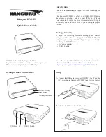
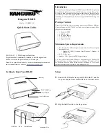
Turn off VF66B (DC motor drive), open the front cover, and connect the current power supply
between (AIN1) and (GND) terminals of the terminal block [TB1] on the control print board
[VFC66-Z] using the Phillips screwdriver (M3).
Warning
[Installing current power supply]
●
Be sure to turn off VF66B (DC motor drive) before installing the current power supply.
Otherwise, it can result in a risk of electric shock.
●
Be sure to turn off VF66B (DC motor drive) before switching.
Otherwise, it can result in a risk of electric shock.
Control print board
[VFC66-Z]
terminal block [TB1]
- After power-on, select "Vin" using [
↑
][
↓
] keys.
- Turn on the current power supply to cause 20mA of current to be input to the [AIN1] terminal.
- A number is displayed.
With VF66B (DC motor drive) turned off, set the SW1 switch to ON (terminal block side) using
the tips of tweezers or a jig with the very narrow tip (approximately 0.8 mm).
- Adjust the value of "L-01" to set the value of monitor item "Vin" to "10.00".
* The display of monitor item "Vin" can be changed to other items through changing the analog
input monitor display selection (G-16). For details, refer to "4.8. Area G in Chapter 4."
After adjustment, remove the current power supply installed using the Phillips screwdriver (M3).
TB1
CN-SO
CN-SI
RY1
CN3
SW2
SW1
CN4
LED1
52MA
86Aa
86Ab
P
COM
GND
+10
PS
PS
MI3
GND
GND
52MA
86A
MO1
MO2
AOT1
AIN1
ST-F
MI1
MI2
MI4
MI5
CN5
3
1
ON
RY2
CN6
SET66-Z
CN7
CN4
VFC66-Z
SW1
AOT1
GND
AIN1
+10