TP7
P 3
5
+~"
WRITE
PROTECT
L.E.D.
I U
2
U29
36
IgO
WRITE
PROTECT
WRPROT-
WRITE+
'2
05V
+ V
5 RP4
4.7K,
PROTECT
SENMR
I
M'539
V3?
RP2
22lC.
s
ZZK
4 7 O Kr
RP2
RP3
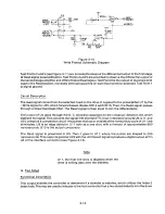
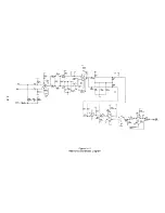
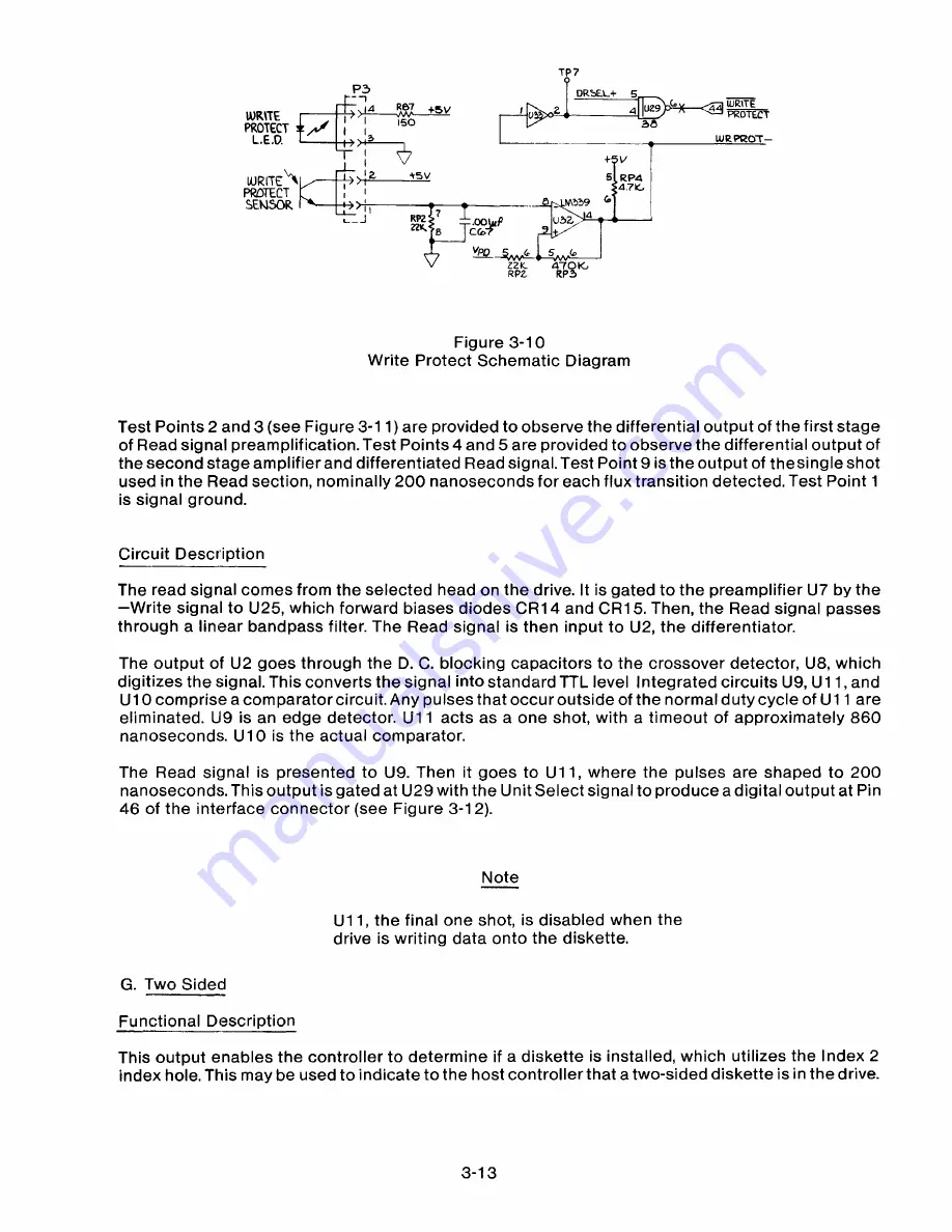
Figure 3-10
Write Protect Schematic Diagram
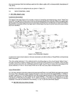
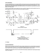
Test Points 2 and 3 (see Figure 3-11) are provided to observe the differential output of the first stage
of Read signal preamplification. Test Points 4 and 5 are provided to observe the differential output of
the second stage amplifier and differentiated Read signal. Test Point 9 is the output of thesingle shot
used in the Read section, nominally 200 nanoseconds for each flux transition detected. Test Point 1
is signal ground.
Circuit Description
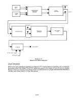
The read signal comes from the selected head on the drive. It is gated to the preamplifier U7 by the
— Write signal to U25, which forward biases diodes CR14 and CR15. Then, the Read signal passes
through a linear bandpass filter. The Read signal is then input to U2, the differentiator.
The output of U2 goes through the D. C. blocking capacitors to the crossover detector, U8, which
digitizes the signal. This converts the signal into standard TTL level Integrated circuits U9, U11, and
U10 comprise a
corn parator
c
ircuit. Any pulses that occur outside of the normal duty cycle of U11 are
eliminated. U9 is an edge det ector. U11 acts as a one shot, with a timeout of approximately 860
nanoseconds. U10 is the actual comparator.
T he Read signal is p resented to U9 . Then it g oe s t o U 1 1 , where th e p u lses are s haped to 2 0 0
nanoseconds. This output is gated at U29 with the Unit Select signal to produce a digital output at Pin
46 of the interface connector (see Figure 3-12).
Note
U11, the final one shot, is disabled when the
drive is writing data onto the diskette.
G. Two Sided
Functional Description
This output enables the controller to determine if a diskette is installed, which utilizes the Index 2
index hole. This may be used to indicate to the host controller that a two-sided diskette is in the drive.
3-1 3
Содержание TM848-1
Страница 32: ...HUB CENTER LINE TRACK 0 TRACK 38 TRACK 76 Figure 2 2 Hub Center Line and Track Locations 2 3 ...
Страница 81: ...APPENDIX I PRINTED CIRCUIT BOARD S CHEM A T ICS AND ASSEM B LY DRAW IN G S ...
Страница 88: ...APPENDIX II RECOM M E N D E D SPARE PARTS LIST ...
Страница 90: ...Pi N 1 79031 001 1 082 ...

