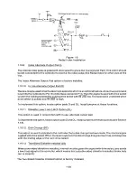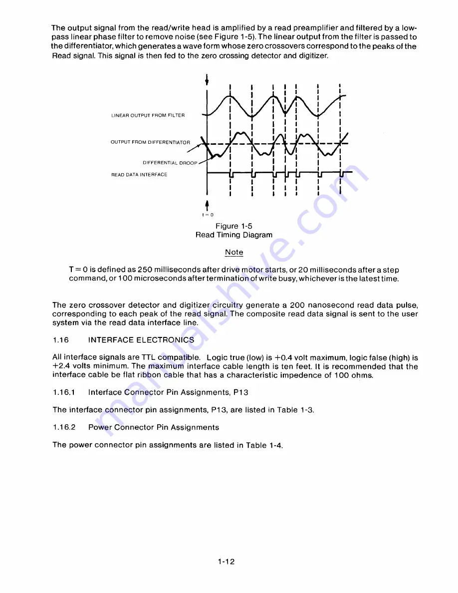
The output signal from the read/write head is amplified by a read preamplifier and filtered by a low-
pass linear phase filter to remove noise (see Figure 1-5). The linear output from the filter is passed to
the differentiator, which generates a wave form whose zero crossovers correspond to the peaks of the
Read signal. This signal is then fed to the zero crossing detector and digitizer.
I
I
I
I
I
I
I I
I I
LINEAR OUTPUT FROM FILTER
I
I
I
I
OUTPUT FROM DIFFERENTIATOR
I
I
I
I
I
I
I
DIFFERENTIAL DROO P
READ DATA INTERFACE
I
I
I
I
I
I
f
I
I
I
I
I
>
I
I = o
Figure 1-5
Read Timing Diagram
Note
T = 0 is defined as 250 milliseconds after drive motor starts, or 20 milliseconds after a step
command, or 100 microseconds after termination of write busy, whichever is the latest time.
The zero crossover detector and digitizer circuitry generate a 20 0 n a n o second read data pulse,
corresponding to each peak of the read signal. The composite read data signal is sent to the user
system via the read data interface line.
1.16
I NTER F ACE ELECTRONICS
All interface signals are TTL compatible. L o g ic true (low) is +0.4 volt maximum, logic false (high) is
+2.4 volts minimum. The maximum interface cable length is ten feet. It is recommended that the
interface cable be flat ribbon cable that has a characteristic impedence of 100 o h ms.
1.16.1
Int e r f ac e Co nnector Pin Assignments, P13
The interface connector pin assignments, P13, are listed in Table 1-3.
1.16.2
Pow e r C o n n e ctor Pin Assignments
The power connector pin assignments are listed in Table 1-4.
1-12
Содержание TM848-1
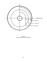
Страница 32: ...HUB CENTER LINE TRACK 0 TRACK 38 TRACK 76 Figure 2 2 Hub Center Line and Track Locations 2 3 ...
Страница 81: ...APPENDIX I PRINTED CIRCUIT BOARD S CHEM A T ICS AND ASSEM B LY DRAW IN G S ...
Страница 88: ...APPENDIX II RECOM M E N D E D SPARE PARTS LIST ...
Страница 90: ...Pi N 1 79031 001 1 082 ...


