NOVA electronics Inc. MCX514 -
156
-
156
-
■
Write data
Then, perform data writing. The data for writing is transmitted from WRn register specified by the slave address, byte by byte.
From only one byte to multiple bytes continuously can be written. In the 9th SCL after sending 1 byte, if MCX514 correctly
receives, it returns ACK signal of Low level to the SDA line. When the CPU receives this ACK signal, then, sends 1 byte data to
be written in the next register address.
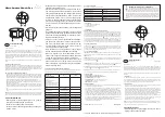
Fig. 4.2-2 Data Writing
■
Generate stop condition
To stop data writing, the user needs to generate stop condition. When SCL signal is Hi and SDA signal changes from Low to Hi, it
becomes stop condition. Whenever sending and receiving, the host CPU must generate this stop condition at the end.
4.2.2 Reading Operation
MCX514 Reading procedures from RR register are described below.
■
Generate start condition
When SCL signal is Hi and SDA signal changes from Hi to Low, it becomes start condition. Whenever sending and receiving, the
host CPU must generate this start condition at the beginning.
■
Write slave address
After making start condition, the user transmits an instruction whether to read from which RR register of which chip to MCX514.
It transmits 8-bit slave address synchronized with SCL shown below, and receives ACK (Low) from MCX514 in the 9th bit. The
slave address is composed of chip address of 3 bits D7
~
D5, register address of 4 bits D4
~
D1 and the bit D0 for reading /
writing.
Fig. 4.2-3 Slave Address
W
ACK
1
2
3
4
5
6
7
8
9
1
2
3
4
5
6
7
8
9
ACK
D7 D6 D5 D4 D3 D2 D1 D0
D7 D6 D5 D4 D3 D2 D1 D0
1
2
3
4
5
6
7
8
9
ACK
Writing data of
register address n
Writing data of
register address n+1
Slave address
Start
Stop
SCL
SDA
SCL
SDA
1
2
3
4
5
6
7
8
9
CA2
CA1
CA0
RA3
RA2
RA1
RA0
Chip address
Register address
ACK
Start
Condition
D7
D0
D5
D4
D1
D6
D3
D2
ACK: 0(Low)
;
outputted by MCX514
Reading
:
1(Hi), Writing
:
0(Low)
R/W


