Semiconductor Group
1-6
1997-10-01
Introduction
C541U
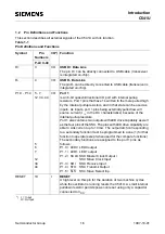
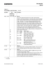
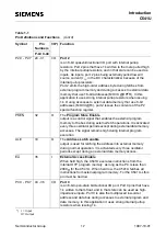
P3.0 - P3.7
11, 13 - 19
11
13
14
15
16
17
18
19
I/O
Port 3
is an 8-bit quasi-bidirectional I/O port with internal pullup
resistors. Port 3 pins that have 1’s written to them are pulled high
by the internal pullup resistors, and in that state can be used as
inputs. As inputs, port 3 pins being externally pulled low will
source current (
I
IL
, in the DC characteristics) because of the
internal pullup resistors. Port 3 also contains the interrupt, timer,
serial port and external memory strobe pins that are used by
various options. The pin with LED drive capability is able to sink
current up to 10 mA. The output latch corresponding to a
secondary function must be programmed to a one (1) for that
function to operate. The secondary functions are assigned to the
pins of port 3, as follows:
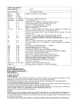
P3.0 / LED2
LED2 output
P3.1 / DADD
Device attached input
P3.2 / INT0
External interrupt 0 input /
timer 0 gate control input
P3.3 / INT1
External interrupt 1 input /
timer 1 gate control input
P3.4 / T0
Timer 0 counter input
P3.5 / T1
Timer 1 counter input
P3.6 / WR
WR control output; latches the
data byte from port 0 into the
external data memory
P3.7 / RD
RD control output; enables the
external data memory
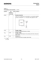
XTAL2
20
–
XTAL2
is the output of the inverting oscillator amplifier. This pin is used
for the oscillator operation with crystal or ceramic resonator.
XTAL1
21
–
XTAL1
is the input to the inverting oscillator amplifier and input to the
internal clock generator circuits.
To drive the device from an external clock source, XTAL1 should
be driven, while XTAL2 is left unconnected.
Minimum and
maximum high and low times as well as rise/fall times specified in
the AC characteristics must be observed.
*) I = Input
O = Output
Table 1-1
Pin Definitions and Functions (cont’d)
Symbol
Pin
Numbers
I/O*) Function
P-LCC-44
Summary of Contents for C541U
Page 1: ... 8 LW 026 0LFURFRQWUROOHU 8VHU V 0DQXDO http www siem ens d Sem iconductor ...
Page 7: ......
Page 21: ...Semiconductor Group 2 6 1997 10 01 Fundamental Structure C541U ...
Page 37: ...Semiconductor Group 4 6 1997 10 01 External Bus Interface C541U ...
Page 133: ...Semiconductor Group 6 88 1999 04 01 On Chip Peripheral Components C541U ...
Page 163: ...Semiconductor Group 8 8 1997 10 01 Fail Safe Mechanisms C541U ...
Page 185: ...Semiconductor Group 10 14 1997 10 01 OTP Memory Operation C541U ...

