Semiconductor Group
9-6
1997-10-01
Power Saving Modes
C541U
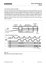
9.2.1 Entering Power Down Mode
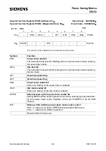
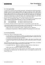
The power down mode is entered by two consecutive instructions. The first instruction has to set the
flag bit PDE (PCON.1) and must not set bit PDS (PCON.6), the following instruction has to set the
start bit PDS (PCON.6) and must not set bit PDE (PCON.1). The hardware ensures that a
concurrent setting of both bits, PDE and PDS, does not initiate the power down mode. Bits PDE and
PDS will automatically be cleared after having been set and the value shown by reading one of
these bits is always 0. This double instruction is implemented to minimize the chance of
unintentionally entering the power down mode which could possibly ”freeze” the chip's activity in an
undesired status. Important : the USB module must be switched off from the system clock prior to
enabling the power down mode by software :
PCON is not a bit-addressable register, so the above mentioned sequence for entering the power-
down mode is obtained by byte-handling instructions, as shown in the following example:
ANL
DCR,#11111101B
;clear bit UCLK; USB clock is switched off
ANL
DCR,#11111110B
;clear bit PCLK, stop PLL (required only in full speed mode)
ORL
PCON,#00000010B
;set bit PDE, bit PDS must not be set
ORL
PCON,#01000000B
;set bit PDS, bit PDE must not be set, enter power-down
The instruction that sets bit PDS is the last instruction executed before going into power down
mode. When the double instruction sequence shown above is used and when bit EWPD in SFR
PCON1 is 0, the power down mode can only be left by a reset operation.
If the wake-up from power down capability is required, its function must be enabled prior to
executing the double instruction sequence shown above.
ORL
SYSCON,#00010000B
;set RMAP
ORL
PCON1,#80H
;enable wake-up from power-down by setting EWPD
;80H = wake-up through pin P3.2/INT0
;90H = wake-up through USB bus
ANL
SYSCON,#11101111B
;reset RMAP (for future SFR accesses)
Note :Before entering the power down mode, the port latch of SFR P3.2 (P3.2/INT0 pin) should
contain a “1“ (pin operates as input). Otherwise, the wake-up sequence discussed in the next
chapter will be started immediately when power down mode is entered.
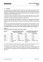
If the wake-up from software power down mode through USB bus capability is selected, the USB
receiver must be enabled in order to detect any activity on the USB bus lines. Therefore, bit RPWD
in the USB device power down register DPWDR must be cleared before enering software power
down mode.
The USB module enters the suspend state when it detects no activity on the USB bus for more than
6 ms.
Summary of Contents for C541U
Page 1: ... 8 LW 026 0LFURFRQWUROOHU 8VHU V 0DQXDO http www siem ens d Sem iconductor ...
Page 7: ......
Page 21: ...Semiconductor Group 2 6 1997 10 01 Fundamental Structure C541U ...
Page 37: ...Semiconductor Group 4 6 1997 10 01 External Bus Interface C541U ...
Page 133: ...Semiconductor Group 6 88 1999 04 01 On Chip Peripheral Components C541U ...
Page 163: ...Semiconductor Group 8 8 1997 10 01 Fail Safe Mechanisms C541U ...
Page 185: ...Semiconductor Group 10 14 1997 10 01 OTP Memory Operation C541U ...

