


Semiconductor Group
6-40
1999-04-01
On-Chip Peripheral Components
C541U
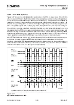
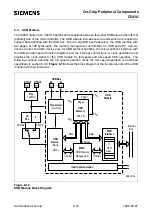
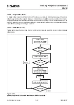
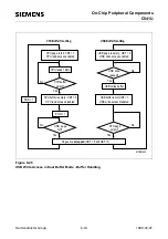
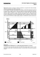
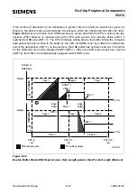
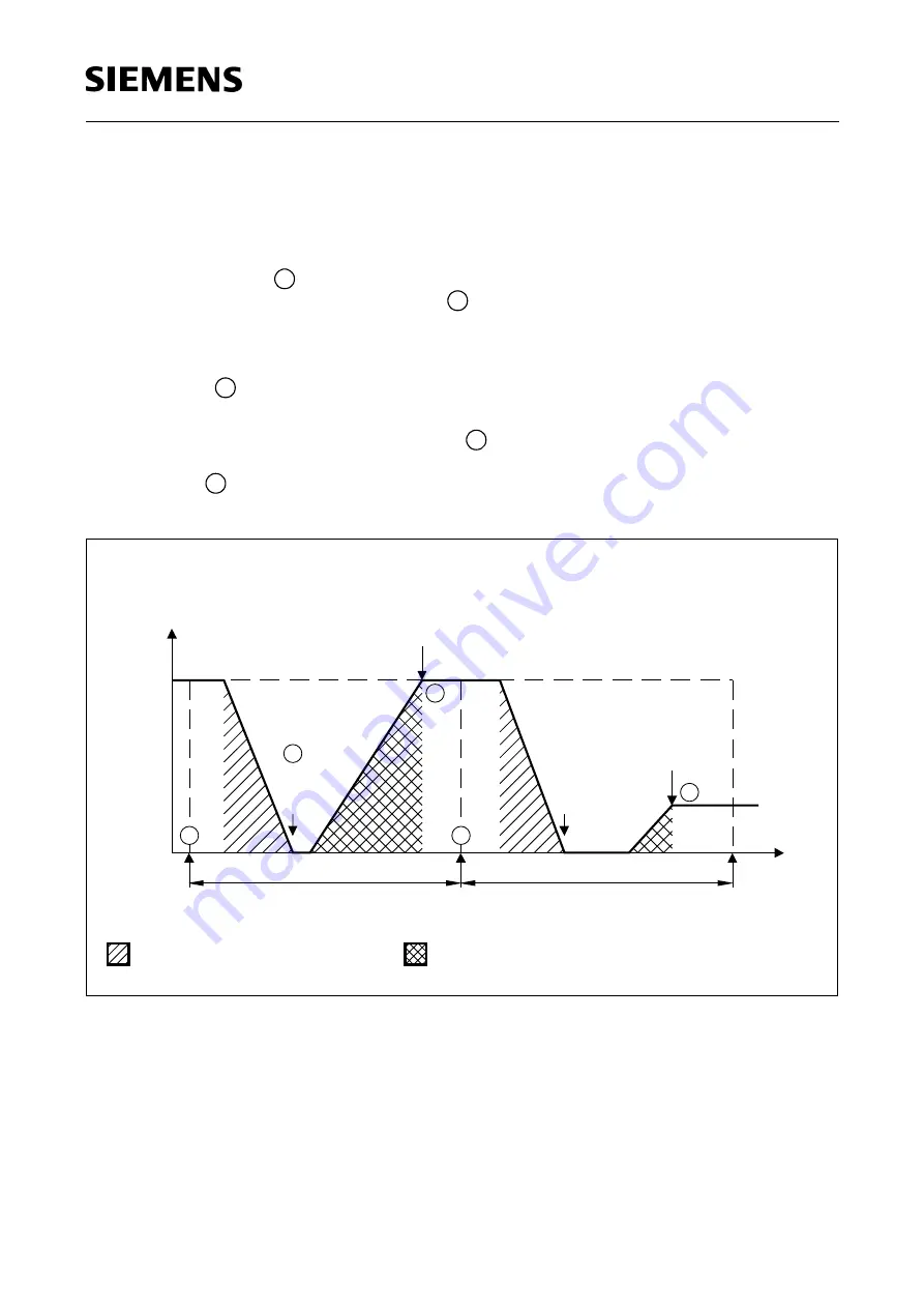
The standard USB read access as shown in figure 6-23 supports random and sequential CPU
access mode of the USB memory. The memory buffer full condition is true when a predefined
number of bytes (MaxLen) has been written by the CPU or when bit DONE has been set by
software.
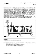
After SOF(n) occured at
with a full USB memory buffer, the USB reads the buffer. Bit SOD is set
at the end of the USB buffer read operation at
, indicating an empty USB memory buffer. Now,
the CPU can write again data into the USB memory buffer until a determined number (MaxLen) of
bytes are transfered or until bit DONE has been set by software. The MaxLen value must be
previously set by software. When the actual USB memory buffer address offset is equal to MaxLen,
bit EOD is set at
to indicate a full buffer. The USB memory buffer address offset is automatically
incremented with every CPU write access to USB memory buffer if bit INCE is set.
During the next frame (after SOF(n+1)) is set at
) the USB memory buffer can be read by the
USB. Bit SOD is set again when the USB memory buffer becomes empty again. If bit DONE is set
by the CPU (at
), the buffer is declared by the CPU to be full, even if the address offset does not
reach the value of MaxLen.
Figure 6-23
Single Buffer Mode : Standard USB Read Access
1
2
3
4
5
1
EOD
set
Frame n
Frame n+1
DONE
set
Time
SOF (n)
set
Number of
Data Bytes
in USB Buffer
MaxLen
USB read accesses
CPU write accesses
MCT03403
2
3
5
SOD
set
SOF (n+2)
set
set
SOF (n+1)
4
set
SOD
Summary of Contents for C541U
Page 1: ... 8 LW 026 0LFURFRQWUROOHU 8VHU V 0DQXDO http www siem ens d Sem iconductor ...
Page 7: ......
Page 21: ...Semiconductor Group 2 6 1997 10 01 Fundamental Structure C541U ...
Page 37: ...Semiconductor Group 4 6 1997 10 01 External Bus Interface C541U ...
Page 133: ...Semiconductor Group 6 88 1999 04 01 On Chip Peripheral Components C541U ...
Page 163: ...Semiconductor Group 8 8 1997 10 01 Fail Safe Mechanisms C541U ...
Page 185: ...Semiconductor Group 10 14 1997 10 01 OTP Memory Operation C541U ...