Semiconductor Group
5-7
1997-10-01
Reset / System Clock
C541U
After a hardware reset operation bits PCLK, SPEED, and UCLK are set to 0. Depending on the
required operating mode of the USB module a well defined procedure must be executed for
switching on the clock for the USB module :
– Full speed mode
USB PLL is switched on by setting bit PCLK
waiting 3 ms for PLL being locked
setting bit UCLK
– Low speed mode
setting bit UCLK only
The switch-on procedure after hardware reset assures a proper operation of the USB clock system.
A software reset operation of the USB module must follow this clock system switch-on procedure.
Details of the software reset operation are described in chapter 6.4.5 on page 6-51.
XTAL1 and XTAL2 are the input and output of a single-stage on-chip inverter which can be
configured with off-chip components as a Pierce oscillator. The oscillator, in any case, drives the
internal clock generator. The clock generator provides the internal clock signals to the chip. These
signals define the internal phases, states and machine cycles.
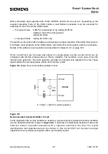
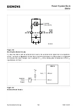
Figure 5-5 shows the recommended oscillator circuit.
Figure 5-5
Recommended Crystal Oscillator Circuit
In this application the on-chip oscillator is used as a crystal-controlled, positive-reactance oscillator
(a more detailed schematic is given in figure 5-6). lt operates in fundamental response mode as an
inductive reactor in parallel resonance with a capacitor external to the chip. The crystal
specifications and capacitances are non-critical. In this circuit 20 pF can be used as single
capacitance at any frequency together with a good quality crystal.
XTAL1
XTAL2
C
C
12
MHz
C = 20pF
±
10pF for crystal operation
C541U
Summary of Contents for C541U
Page 1: ... 8 LW 026 0LFURFRQWUROOHU 8VHU V 0DQXDO http www siem ens d Sem iconductor ...
Page 7: ......
Page 21: ...Semiconductor Group 2 6 1997 10 01 Fundamental Structure C541U ...
Page 37: ...Semiconductor Group 4 6 1997 10 01 External Bus Interface C541U ...
Page 133: ...Semiconductor Group 6 88 1999 04 01 On Chip Peripheral Components C541U ...
Page 163: ...Semiconductor Group 8 8 1997 10 01 Fail Safe Mechanisms C541U ...
Page 185: ...Semiconductor Group 10 14 1997 10 01 OTP Memory Operation C541U ...

