Semiconductor Group
3-7
1997-10-01
Memory Organization
C541U
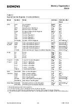
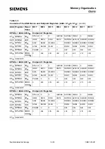
ACH
SCIEN
XXXX-
XX00B
–
–
–
–
–
–
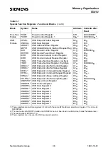
WCEN TCEN
B0H
2)
P3
FFH
RD
WR
T1
T0
INT1
INT0
DADD
LED2
B1H SYSCON XX10-
XXXXB
–
–
EALE
RMAP
–
–
–
–
B8H
2)
IP0
XXXX-
0000B
–
–
–
–
PT1
PX1
PT0
PX0
B9H IP1
XXXX-
X000B
–
–
–
–
–
PUDI
PUEI
PSSC
C0H
2)
WDCON
XXXX-
0000B
–
–
–
–
OWDS WDTS
WDT
SWDT
C1H to C7H
USB Device and Endpoint Register definition see table 3-3
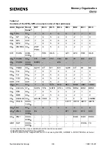
D0H
2)
PSW
00H
CY
AC
F0
RS1
RS0
OV
F1
P
D2H EPSEL
80H
EPS7
0
0
0
0
EPS2
EPS1
EPS0
D3H USBVAL 00H
.7
.6
.5
.4
.3
.2
.1
.0
D4H ADROFF 00H
6)
0
0
AO5
AO4
AO3
AO2
AO1
AO0
D6H GEPIR
00H
DRVI
0
0
EPI4
EPI3
EPI2
EPI1
EPI0
E0H
2)
ACC
00H
.7
.6
.5
.4
.3
.2
.1
.0
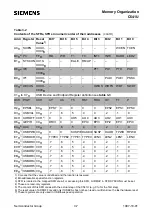
E6H
7)
USBPWD 00H
0
0
SUSPIE DADDIE SUSP
DADD
TPWD
RPWD
E7H
7)
USBDCR 00H
TYPE3 TYPE2 TYPE1 TYPE0 LEN3
LEN2
LEN1
LEN0
E8H
7)
USBDR0 00H
.7
.6
.5
.4
.3
.2
.1
.0
E9H
7)
USBDR1 00H
.7
.6
.5
.4
.3
.2
.1
.0
EAH
7)
USBDR2 00H
.7
.6
.5
.4
.3
.2
.1
.0
EBH
7)
USBDR3 00H
.7
.6
.5
.4
.3
.2
.1
.0
ECH
7)
USBDR4 00H
.7
.6
.5
.4
.3
.2
.1
.0
EDH
7)
USBDR5 00H
.7
.6
.5
.4
.3
.2
.1
.0
EEH
7)
USBDR6 00H
.7
.6
.5
.4
.3
.2
.1
.0
1) X means that the value is undefined and the location is reserved
2) Bit-addressable special function registers
3) SFR is located in the mapped SFR area. For accessing this SFR, bit RMAP in SFR SYSCON must be set.
4) These are read-only registers
5) The content of this SFR varies with the actual step of the C541U (e.g. 01
H
for the first step)
6) The reset value of ADROFF is valid only if USBVAL has not been read or written since the last hardware reset
7) These registers are only used in USB low-speed operation.
Table 3-2
Contents of the SFRs, SFRs in numeric order of their addresses (cont’d)
Addr Register Reset
Value
1)
Bit 7
Bit 6
Bit 5
Bit 4
Bit 3
Bit 2
Bit 1
Bit 0
Summary of Contents for C541U
Page 1: ... 8 LW 026 0LFURFRQWUROOHU 8VHU V 0DQXDO http www siem ens d Sem iconductor ...
Page 7: ......
Page 21: ...Semiconductor Group 2 6 1997 10 01 Fundamental Structure C541U ...
Page 37: ...Semiconductor Group 4 6 1997 10 01 External Bus Interface C541U ...
Page 133: ...Semiconductor Group 6 88 1999 04 01 On Chip Peripheral Components C541U ...
Page 163: ...Semiconductor Group 8 8 1997 10 01 Fail Safe Mechanisms C541U ...
Page 185: ...Semiconductor Group 10 14 1997 10 01 OTP Memory Operation C541U ...

