Semiconductor Group
6-49
1999-04-01
On-Chip Peripheral Components
C541U
6.4.3 USB Memory Buffer Organization
The address generation of the USB memory buffer is based on address offset and base address
pointer. This scheme allows flexible and application specific buffer allocation and management. The
length of an endpoint buffer can be up to 8, 16, 32, or 64 bytes. The start address of each endpoint
buffer can be located to memory locations according table 6-5.
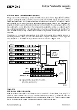
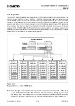
In order to avoid unused memory space between two endpoint buffers, the largest buffer should be
located at the highest address. This structure should be used to allocate USB memory for all
endpoint buffers. The base address for the setup packet is always located at address 00
H
. This
leads to a typical USB buffer structure as shown in figure 6-31 with a buffer length of 64 bytes for
endpoint 2, 16 bytes for endpoints 1 and 3, 8 bytes for endpoint 0, and a predefined length of 8 bytes
for endpoint 0 and the setup token.
Figure 6-31
Endpoint Buffer Allocation (Example: 4 Endpoints)
Table 6-5
USB Buffer Length and Base Addresses Values
Buffer Length
Valid Buffer Base Addresses
8 bytes
08H, 10H, 18H, 20H, 28H, 30H, 38H, 40H, 48H, 50H, 58H, 60H, 68H, 70H, 78H
16 bytes
10H, 20H, 30H, 40H, 50H, 60H, 70H
32 bytes
20H, 40H, 60H
64 bytes
40H
Endpoint 2 Buffer
Endpoint 2 Buffer
Endpoint 3 Buffer
Endpoint 1 Buffer
Setup Token
40
H
Buffer Block
EPBAn
EPLENn
Endpoint 2
EPBA2=08H EPLEN2=40H
Endpoint 3
EPBA3=06H EPLEN3=10H
Endpoint 1
EPBA1=04H EPLEN1=10H
Endpoint 0
EPBA0=03H EPLEN0=08H
Setup Token
Adress 00H
on page 0
8 Bytes
7F
H
30
H
20
H
18
H
00
H
Endpoint 0 Buffer
Summary of Contents for C541U
Page 1: ... 8 LW 026 0LFURFRQWUROOHU 8VHU V 0DQXDO http www siem ens d Sem iconductor ...
Page 7: ......
Page 21: ...Semiconductor Group 2 6 1997 10 01 Fundamental Structure C541U ...
Page 37: ...Semiconductor Group 4 6 1997 10 01 External Bus Interface C541U ...
Page 133: ...Semiconductor Group 6 88 1999 04 01 On Chip Peripheral Components C541U ...
Page 163: ...Semiconductor Group 8 8 1997 10 01 Fail Safe Mechanisms C541U ...
Page 185: ...Semiconductor Group 10 14 1997 10 01 OTP Memory Operation C541U ...

