Semiconductor Group
5-2
1997-10-01
Reset / System Clock
C541U
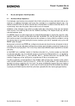
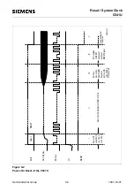
Figure 5-1
Reset Circuitries
A correct reset leaves the processor in a defined state. The program execution starts at location
0000H. After reset is internally accomplished the port latches of ports 0 to 3 are set to FFH. This
leaves port 0 floating, since it is an open drain port when not used as data/address bus. All other I/
O port lines (ports 1 and 3) output a one (1). Port 2 lines output a zero (or one) after reset, if EA is
held low (or high).
The content of the internal RAM of the C541U is not affected by a reset. After power-up the content
is undefined, while it remains unchanged during a reset if the power supply is not turned off.
A reset operation of the USB module in the C541U can only be achieved under software control. A
hardware reset operation puts only the internal CPU interface of the USB module and its MMU into
a well defined reset state.
The software reset, which must be executed after a hardware reset, is initiated by setting bit SWR
in SFR DCR by software. Bit SWR is reset automatically by hardware when the software reset
operation of the USB module is finished. Further, with the reset of bit SWR, bit DINIT in DCR is set
indicating the CPU that it has to initialize the endpoints of USB module.
RESET
+
a)
RESET
b)
&
RESET
c)
V
DD
+
V
DD
V
DD
C541U
C541U
C541U
Summary of Contents for C541U
Page 1: ... 8 LW 026 0LFURFRQWUROOHU 8VHU V 0DQXDO http www siem ens d Sem iconductor ...
Page 7: ......
Page 21: ...Semiconductor Group 2 6 1997 10 01 Fundamental Structure C541U ...
Page 37: ...Semiconductor Group 4 6 1997 10 01 External Bus Interface C541U ...
Page 133: ...Semiconductor Group 6 88 1999 04 01 On Chip Peripheral Components C541U ...
Page 163: ...Semiconductor Group 8 8 1997 10 01 Fail Safe Mechanisms C541U ...
Page 185: ...Semiconductor Group 10 14 1997 10 01 OTP Memory Operation C541U ...

