Semiconductor Group
9-8
1997-10-01
Power Saving Modes
C541U
When the power-down mode wake-up capability has been enabled (bit EWPD in SFR PCON1 set)
prior to entering power down mode, the power down mode can be exit either via P3.2/INT0 or an
activity on the USB bus.
9.2.2.1
Exit via Pin P3.2/INT0
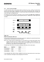
The following procedure :
1. In power down mode pin INT0 must be held at high level.
2. Power down mode is left when INT0 goes low. With INT0 = low the internal RC oscillator is
started. INT0 is then latched by the RC oscillator clock signal. Therefore, INT0 should be held at
low level for at least 10
µ
s (latch phase). After this delay INT0 can be set again to high level if
required. Thereafter, the oscillator watchdog unit controls the wake-up procedure in its start-up
phase.
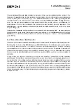
3. The oscillator watchdog unit starts its operation. When the on-chip oscillator clock is detected for
stable nominal frequency, the microcontroller further waits for a delay of typically 5 ms and then
starts again with its operation initiating the power down wake-up interrupt. The interrupt address
of the first instruction to be executed after wake-up is 007BH.
4. The clock system of the USB module must be setup again by software : USB PLL is switched on
by setting bit PCLK in SFR DCR.(only required in full speed mode); Therafter, the PLL must be
stabilized by waiting typically 3 ms. Now bit UCLK in SFR DCR can be set.
5. After the RETI instruction of the power down wake-up interrupt routine has been executed, the
instruction which follows the initiating power down mode double instruction sequence will be
executed. The peripheral units timer 0/1, SSC, and WDT are frozen until end of phase 4.
All interrupts of the C541U are disabled from phase 2) until the end of phase 4). Other Interrupts
can be first handled after the RETI instruction of the wake-up interrupt routine.
Depending on the requirements, point 4 can also be executed in pahse 5) after the execution of the
RETI instruction described in point 5 above.
9.2.2.2
Exit via UBS Bus
If the wake-up from software power down mode through USB bus capability has been selected, any
activity on the USB bus causes the termination of the suspend state, triggers the watchdog unit and
starts the wake-up procedure. After the start trigger by the USB bus activity, the actions 3. to 5. as
described above are executed.
The wake-up trigger signal from the USB module can only be generated if the USB receiver circuitry
was enabled in software power down mode.
Summary of Contents for C541U
Page 1: ... 8 LW 026 0LFURFRQWUROOHU 8VHU V 0DQXDO http www siem ens d Sem iconductor ...
Page 7: ......
Page 21: ...Semiconductor Group 2 6 1997 10 01 Fundamental Structure C541U ...
Page 37: ...Semiconductor Group 4 6 1997 10 01 External Bus Interface C541U ...
Page 133: ...Semiconductor Group 6 88 1999 04 01 On Chip Peripheral Components C541U ...
Page 163: ...Semiconductor Group 8 8 1997 10 01 Fail Safe Mechanisms C541U ...
Page 185: ...Semiconductor Group 10 14 1997 10 01 OTP Memory Operation C541U ...

