


Semiconductor Group
6-54
1999-04-01
On-Chip Peripheral Components
C541U
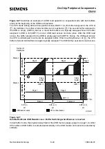
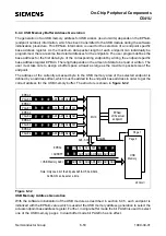
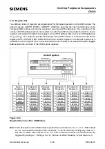
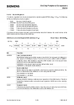
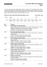
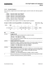
6.4.7 Register Set
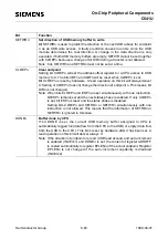
Two different kinds of registers are implemented for full speed operation in the USB module. The
global registers (GEPIR, EPSEL, ADROFF, USBVAL) describe the basic functionality of the
complete USB module and can be accessed via unique SFR addresses. For reduction of the
number of SFR addresses which are needed to control the USB module inside the C541U, device
registers and endpoint registers are mapped into an SFR address block of seven SFR addresses
(C1H to C7H). The endpoint specific functionality of the USB module is controlled via the device
registers DCR, DPWDR, DIER, DIRR and the frame number registers. An endpoint register set is
available for each endpoint (n=0..4) and describes the functionality of the selected endpoint. Figure
6-34 explains the structure of the USB module registers.
Figure 6-34
Register Structure of the USB Module
Note: In the description of the USB module registers bits are marked as “rw“, “r“, or “w“. Bits marked
as “rw“ can be read and written. Bits marked as “r“ can be read only. Writing any value to “r“
bits has no effect. Bits marked as “w“ are used to execute internal commands which are
triggered by writing a 1. Writing a 0 to “w“ bits has no effect. Reading “w“ bits returns a 0.
D
Global Registers
EPSEL(D2
H
)
Endpoint 0
Registers
EPBC0
EPBS0
EPIE0
EPIR0
EPBA0
EPLEN0
C1
H
C2
H
C3
H
C4
H
C5
H
C6
H
C7
H
reserved
Endpoint 1
Registers
EPBC1
EPBS1
EPIE1
EPIR1
EPBA1
EPLEN1
C1
H
C2
H
C3
H
C4
H
C5
H
C6
H
C7
H
reserved
Endpoint 2
Registers
EPBC2
EPBS2
EPIE2
EPIR2
EPBA2
EPLEN2
C1
H
C2
H
C3
H
C4
H
C5
H
C6
H
C7
H
reserved
Endpoint 3
Registers
EPBC3
EPBS3
EPIE3
EPIR3
EPBA3
EPLEN3
C1
H
C2
H
C3
H
C4
H
C5
H
C6
H
C7
H
reserved
Endpoint 4
Registers
EPBC4
EPBS4
EPIE4
EPIR4
EPBA4
EPLEN4
C1
H
C2
H
C3
H
C4
H
C5
H
C6
H
C7
H
reserved
Device
Registers
DCR
DIER
DIRR
FNRL
C1
H
C2
H
C3
H
C4
H
C5
H
C6
H
C7
H
reserved
DPWDR
FNRH
.0
.1
.2
.7
USBVAL(D3
H
)
ADROFF(D4
H
)
GEPIR(D6
H
)
.0
.1
.2
.7 .6 .5 .4 .3
.0
.1
.2
.4 .3
.5
.0
.1
.2
.4 .3
0 0
0 0
0 0 0 0
Decoder
Summary of Contents for C541U
Page 1: ... 8 LW 026 0LFURFRQWUROOHU 8VHU V 0DQXDO http www siem ens d Sem iconductor ...
Page 7: ......
Page 21: ...Semiconductor Group 2 6 1997 10 01 Fundamental Structure C541U ...
Page 37: ...Semiconductor Group 4 6 1997 10 01 External Bus Interface C541U ...
Page 133: ...Semiconductor Group 6 88 1999 04 01 On Chip Peripheral Components C541U ...
Page 163: ...Semiconductor Group 8 8 1997 10 01 Fail Safe Mechanisms C541U ...
Page 185: ...Semiconductor Group 10 14 1997 10 01 OTP Memory Operation C541U ...