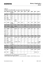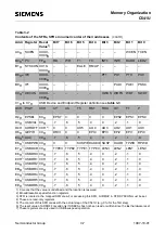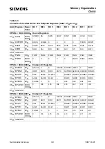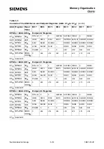
Semiconductor Group
2-5
1997-10-01
Fundamental Structure
C541U
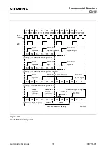
Figure 2-2
Fetch Execute Sequence
S1
P1 P2 P1 P2
S2
P1 P2 P1 P2
S3
S4
P1 P2 P1 P2
S5
S6
P1 P2 P1 P2
S1
S2
P1 P2 P1 P2
S3
S4
P1 P2 P1 P2
S5
S6
OSC
(XTAL2)
ALE
Read
Opcode
Read Next
Opcode (Discard)
S1
S2
S3
S4
S5
S6
(a) 1-Byte, 1-Cycle Instruction, e. g. INC A
Opcode Again
Read Next
(b) 2-Byte, 1-Cycle Instruction, e. g. ADD A #DATA
Read
Opcode
S1
S2
Byte
Read 2nd
S4
S3
S5
S6
Opcode
Read Next
S6
S5
S3
S4
S2
S1
Opcode
Read
Read Next Opcode (Discard)
S1
S2
S4
S3
S5
S6
Read Next
Opcode Again
(c) 1-Byte, 2-Cycle Instruction, e. g. INC DPTR
(d) MOVX (1-Byte, 2-Cycle)
S4
S1
S2
S3
S5
S6
S1
S3
S2
S4
S5
S6
Read
Opcode
(MOVX)
(Discard)
Opcode
Read Next
No Fetch
No ALE
No Fetch
Read Next Opcode Again
ADDR
DATA
Access of External Memory
MCD03287
Summary of Contents for C541U
Page 1: ... 8 LW 026 0LFURFRQWUROOHU 8VHU V 0DQXDO http www siem ens d Sem iconductor ...
Page 7: ......
Page 21: ...Semiconductor Group 2 6 1997 10 01 Fundamental Structure C541U ...
Page 37: ...Semiconductor Group 4 6 1997 10 01 External Bus Interface C541U ...
Page 133: ...Semiconductor Group 6 88 1999 04 01 On Chip Peripheral Components C541U ...
Page 163: ...Semiconductor Group 8 8 1997 10 01 Fail Safe Mechanisms C541U ...
Page 185: ...Semiconductor Group 10 14 1997 10 01 OTP Memory Operation C541U ...

