Semiconductor Group
6-8
1999-04-01
On-Chip Peripheral Components
C541U
6.1.1.3
Port 0 Circuitry
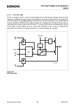
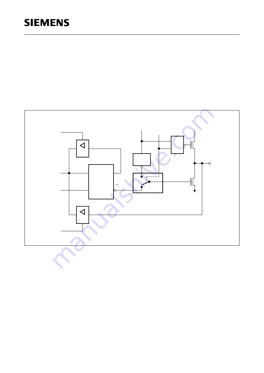
Port 0, in contrast to ports 1, 2 and 3, is considered as "true" bidirectional, because the port 0 pins
float when configured as inputs. Thus, this port differs in not having internal pullups. The pullup FET
in the P0 output driver (see figure 6-6) is used only when the port is emitting 1 s during the external
memory accesses. Otherwise, the pullup is always off. Consequently, P0 lines that are used as
output port lines are open drain lines. Writing a "1" to the port latch leaves both output FETs off and
the pin floats. In that condition it can be used as high-impedance input. If port 0 is configured as
general I/O port and has to emit logic high-level (1), external pullups are required.
Figure 6-6
Port 0 Circuitry
MCS02122
D
CLK
Bit
Latch
Q
Q
Control
Addr./Data
MUX
Read
Latch
to
Latch
Read
Pin
Write
V
CC
Int. Bus
&
Pin
Port
=1
Summary of Contents for C541U
Page 1: ... 8 LW 026 0LFURFRQWUROOHU 8VHU V 0DQXDO http www siem ens d Sem iconductor ...
Page 7: ......
Page 21: ...Semiconductor Group 2 6 1997 10 01 Fundamental Structure C541U ...
Page 37: ...Semiconductor Group 4 6 1997 10 01 External Bus Interface C541U ...
Page 133: ...Semiconductor Group 6 88 1999 04 01 On Chip Peripheral Components C541U ...
Page 163: ...Semiconductor Group 8 8 1997 10 01 Fail Safe Mechanisms C541U ...
Page 185: ...Semiconductor Group 10 14 1997 10 01 OTP Memory Operation C541U ...


