


Semiconductor Group
6-13
1999-04-01
On-Chip Peripheral Components
C541U
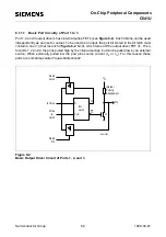
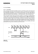
6.1.3.2
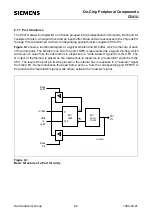
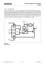
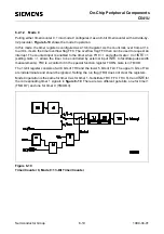
Port Loading and Interfacing
The output buffers of ports 1, 2 and 3 can drive TTL inputs directly. The maximum port load which
still guarantees correct logic output levels can be looked up in the C541U DC characteristics in
chapter 10. The corresponding parameters are
V
OL
and
V
OH
.
The same applies to port 0 output buffers. They do, however, require external pullups to drive
floating inputs, except when being used as the address/data bus.
When used as inputs it must be noted that the ports 1, 2 and 3 are not floating but have internal
pullup transistors. The driving devices must be capable of sinking a sufficient current if a logic low
level shall be applied to the port pin (the parameters
I
TL
and
I
IL
in the C541U DC characteristics
specify these currents). Port 0 has floating inputs when used for digital input.
Summary of Contents for C541U
Page 1: ... 8 LW 026 0LFURFRQWUROOHU 8VHU V 0DQXDO http www siem ens d Sem iconductor ...
Page 7: ......
Page 21: ...Semiconductor Group 2 6 1997 10 01 Fundamental Structure C541U ...
Page 37: ...Semiconductor Group 4 6 1997 10 01 External Bus Interface C541U ...
Page 133: ...Semiconductor Group 6 88 1999 04 01 On Chip Peripheral Components C541U ...
Page 163: ...Semiconductor Group 8 8 1997 10 01 Fail Safe Mechanisms C541U ...
Page 185: ...Semiconductor Group 10 14 1997 10 01 OTP Memory Operation C541U ...