Semiconductor Group
6-3
1999-04-01
On-Chip Peripheral Components
C541U
6.1.1.1
Basic Port Circuirty of Port 1 to 3
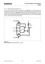
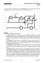
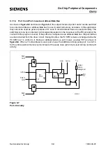
Port 1, 2 and 3 output drivers have internal pullup FET’s (see figure 6-2). Each I/O line can be used
independently as an input or output. To be used as an input, the port bit stored in the bit latch must
contain a one (1) (that means for figure 6-2: Q=0), which turns off the output driver FET n1. Then,
for ports 1, 2 and 3, the pin is pulled high by the internal pullups, but can be pulled low by an external
source. When externally pulled low the port pins source current (
I
IL
or
I
TL
). For this reason these
ports are sometimes called "quasi-bidirectional".
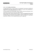
Figure 6-2
Basic Output Driver Circuit of Ports 1, 2, and 3
MCS01823
D
CLK
Bit
Latch
Q
Q
Internal
Pull Up
Arrangement
Pin
Read
Latch
to
Latch
Read
Pin
Write
V
CC
Int. Bus
n1
Summary of Contents for C541U
Page 1: ... 8 LW 026 0LFURFRQWUROOHU 8VHU V 0DQXDO http www siem ens d Sem iconductor ...
Page 7: ......
Page 21: ...Semiconductor Group 2 6 1997 10 01 Fundamental Structure C541U ...
Page 37: ...Semiconductor Group 4 6 1997 10 01 External Bus Interface C541U ...
Page 133: ...Semiconductor Group 6 88 1999 04 01 On Chip Peripheral Components C541U ...
Page 163: ...Semiconductor Group 8 8 1997 10 01 Fail Safe Mechanisms C541U ...
Page 185: ...Semiconductor Group 10 14 1997 10 01 OTP Memory Operation C541U ...

