P746/EN FD/G31
Firmware Design
(FD) 9-
8
MiCOM
P746
FD
2. HARDWARE
MODULES
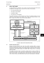
The relay is based on a modular hardware design where each module performs a separate
function within the relay operation. This section describes the functional operation of the
various hardware modules.
2.1 Processor
board
The relay is based around a TMS320VC33 floating point, 32-bit digital signal processor
(DSP) operating at a clock frequency of 75MHz. This processor performs all of the
calculations for the relay, including the protection functions, control of the data
communication and user interfaces including the operation of the LCD, keypad and LEDs.
The processor board is located directly behind the relay’s front panel which allows the LCD,
function keys and LEDs to be mounted on the processor board along with the front panel
communication ports. These comprise the 9-pin D-connector for EIA(RS)232 serial
communications (e.g. using MiCOM S1 V2 or Studio and Courier communications) and the
25-pin D-connector relay test port for parallel communication. All serial communication is
handled using a field programmable gate array (FPGA).
All serial communication is handled using a two-channel 85C30 serial communications
controller (SCC).
The memory provided on the main processor board is split into two categories, volatile and
non-volatile; the volatile memory is fast access SRAM which is used for the storage and
execution of the processor software, and data storage as required during the processor’s
calculations. The non-volatile memory is sub-divided into 2 groups; 4MB of flash memory for
non-volatile storage of software code, present setting values, text, configuration data, latched
data signals (from control inputs, function keys, LEDs, relay outputs) and 4MB of battery
backed-up SRAM for the storage of disturbance, event, fault and maintenance record data.
2.2 Internal
communication
bus
The internal interconnexion bus is controlled by the main board. Via its interconnection bus
the main board controls also the IRIG-B board (if present).
This interconnection bus is based on a 64-way ribbon cable. The ribbon cable carries the
data and address bus signals in addition to control signals and all power supply lines.
Operation of the bus is driven by the main processor board that operates as a master while
all other modules within the relay are slaves.
The DSP processor has a built-in serial port that is used to read the sample data from the
serial bus. The serial bus is also carried on the 64-way ribbon cable.
The main part of the bus is a parallel link with 6 address lines for board selection, 16 data
lines and control lines. On the main controlled bus, main board drive address and control
lines.
Other parts of the buses are:
•
Power supply which are directly wired between the two interconnection buses.
•
Serial lines for rear RS485 communication. So in any way main board keeps control of
the rear RS485 communication.
Summary of Contents for MiCOM P746
Page 4: ......
Page 5: ...Pxxx EN SS G11 SAFETY SECTION...
Page 6: ......
Page 8: ...Pxxx EN SS G11 Page 2 8 Safety Section BLANK PAGE...
Page 16: ...P746 EN IT G31 Introduction MiCOM P746...
Page 18: ...P746 EN IT G31 Introduction IT 1 2 MiCOM P746 IT BLANK PAGE...
Page 26: ...P746 EN TD G31 Technical Data MiCOM P746...
Page 38: ...P746 EN GS G31 Getting Started MiCOM P746...
Page 78: ...P746 EN ST G31 Getting Started MiCOM P746...
Page 80: ...P746 EN ST G31 Settings ST 4 2 MiCOM P746 ST BLANK PAGE...
Page 112: ...P746 EN ST G31 Settings ST 4 34 MiCOM P746 ST BLANK PAGE...
Page 114: ...P746 EN OP G31 Operation MiCOM P746...
Page 136: ...P746 EN OP G31 Operation OP 5 22 MiCOM P746 OP BLANK PAGE...
Page 138: ...P746 EN AP G31 Application Notes MiCOM P746...
Page 142: ...P746 EN AP G31 Application Notes AP 6 4 MiCOM P746 AP BLANK PAGE...
Page 194: ...P746 EN AP G31 Application Notes AP 6 56 MiCOM P746 AP BLANK PAGE...
Page 196: ...P746 EN PL G31 Programmable Logic MiCOM P746...
Page 238: ...P746 EN MR A11 Measurements and Recording MiCOM P746...
Page 240: ...P746 EN MR A11 Measurements and Recording MR 8 2 MiCOM P746 MR BLANK PAGE...
Page 258: ...P746 EN FD G31 Firmware Design MiCOM P746...
Page 280: ......
Page 348: ...P746 EN MT A11 Maintenance MiCOM P746...
Page 350: ...P746 EN MT A11 Maintenance MT 11 2 MiCOM P746 MT BLANK PAGE...
Page 364: ...P746 EN MT A11 Maintenance MT 11 16 MiCOM P746 MT BLANK PAGE...
Page 366: ...P746 EN TS G31 Troubleshooting MiCOM P746...
Page 368: ...P746 EN TS G31 Troubleshooting TS 12 2 MiCOM P746 TS BLANK PAGE...
Page 382: ...P746 EN SC G31 SCADA Communications MiCOM P746...
Page 424: ...P746 EN SC G31 SCADA Communications SC 13 42 MiCOM P746 SC BLANK PAGE...
Page 426: ...P746 EN SG F21 Symbols and Glossary MiCOM P746...
Page 438: ......
Page 440: ...P746 EN IN G31 Installation IN 15 2 MiCOM P746 IN BLANK PAGE...
Page 468: ......
Page 470: ...P746 EN HI G31 Remote HMI HI 16 2 MiCOM P746 HI BLANK PAGE...
Page 500: ...P746 EN HI G31 Remote HMI HI 16 32 MiCOM P746 HI BLANK PAGE...
Page 502: ......
Page 504: ...P746 EN CS A11G31 Cyber Security CS 17 2 MiCOM P746 CS BLANK PAGE...
Page 524: ...P746 EN VH G31 Firmware and Service Manual Version History MiCOM P746...
Page 529: ......


