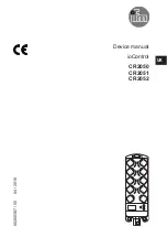
background image

Device manual

ioControl 


CR2050 

CR2051 

CR2052

80268387 / 00


04 / 2018

UK

Original Scale Drawing (MTD)

P_MZ_e100_0092

EPS Source

Product Scale Drawing

Frame Size: 80 mm x 90 mm

30%

333,4%

1

2

4

6

8

3

5

7

205,5

234,2

76

52

17

6,9

8,7

6,9

1

2

3

27,4

11

40,5

4

5

Summary of Contents for ioControl CR2050

Page 1: ...Device manual ioControl CR2050 CR2051 CR2052 80268387 00 04 2018 UK Original P_MZ_e100_0092 30 333 4...

Page 2: ...ies 10 6 3 Frequency inputs 10 6 4 Reverse polarity protection 10 6 5 Supply of the signal generators at the inputs 10 6 6 Fuses 10 6 7 Examples for connection types 11 6 7 1 CR2050 11 6 7 2 CR2051 12...

Page 3: ...d disposal 39 10 1 Maintenance 39 10 2 Cleaning the housing surface 39 10 3 Repair 39 10 4 Disposal 39 11 Approvals standards 39 12 Appendix 40 12 1 EMCY Object 40 12 2 Object directory CR205x 40 12 2...

Page 4: ...keys buttons or indications Cross reference Important note Non compliance may result in malfunction or interference Information Supplementary note WARNING Warning of serious personal injury Death or s...

Page 5: ...ternally before handling it Supply via a mobile on board system 12 24V battery voltage or safety extra low voltage SELV according to the technical data The supply is directly transferred to the connec...

Page 6: ...configure the inputs and outputs to adapt to the respective application The controllers can be used as CANopen slave CANopen master or intelligent I O module 9 Technical data Application specific ext...

Page 7: ...gment display Operating keys More information and accessories at www ifm com 5 Installation 5 1 Mounting surface NOTE The housing must not be exposed to any torsional forces or mechanical stress Mount...

Page 8: ...ta Screws to be used examples Standard Cylinder screws with hexagon socket M5 x L DIN EN ISO 4762 Cylinder screws with hexagon socket and low head M5 x L DIN 7984 5 3 Cable seal NOTE Protection rating...

Page 9: ...ction 2 5 CAN1 OUT 6 X1 Connection cable plug 7 CAN1 IN 8 Connector 1 9 Connector 3 10 Connector 5 11 Connector 7 9 Connector area here e g CR0403 Connector CR2050 CR2051 CR2052 Number of poles 1 IN00...

Page 10: ...ection of the operating voltage CR2051 There is no reverse polarity protection of the CAN supply voltage as this voltage is not used within the device 6 5 Supply of the signal generators at the inputs...

Page 11: ...ppl GNDCAN to the common ground 6 7 Examples for connection types 6 7 1 CR2050 Example 1 CAN loop supply via CAN IN CR2050 Load Dump Protection CAN IN CAN OUT 03 04 VCAN 02 05 CAN1 Supply 3 A n c n c...

Page 12: ...03 04 VCAN CAN1 GNDCAN 03 02 05 CAN2 02 05 01 06 GND GND GND Supply 15 25 A Supply max 25 A CR2051 Load Dump Protection CAN IN CAN OUT 03 04 VCAN 02 05 CAN1 01 06 GNDCAN VBB S VBB 1 06 GND 1 VBB 2 GND...

Page 13: ...1 04 03 04 VCAN CAN1 GNDCAN 03 GND 2 02 05 CAN2 02 05 01 06 Supply 3 A GND GND CR2052 Load Dump Protection CAN IN CAN OUT 03 04 VCAN 02 05 CAN1 01 06 GNDCAN VBB S 06 GND 1 VBB 2 01 04 03 04 VCAN CAN1...

Page 14: ...ellow 2 Power LED green 3 Mode LED green 4 Application LEDs LED A LED D green 5 Lock LED green 6 Diagnostics LED red 7 4 digit 10 segment display Indicators 10 segment display 9 Technical data Origina...

Page 15: ...device is configured as a controller the corresponding menu structure has to be defined see system manual ioControl Node ID uLoc Loc nodE 123 1 1 BAUD Baud rate Error code 1 Error code 2 Error code 3...

Page 16: ...Hz Fault at the input 9 voltage input 32 V Off 10 digital input BL Off Input signal FALSE On Input signal TRUE 11 digital input BL mit Diagnose Off Input signal FALSE On Input signal TRUE 2 Hz Fault...

Page 17: ...vice displays error code 1 if applicable Press the DOWN button again Every time the DOWN button is pressed the device displays another error code if applicable Use the UP button to go back Max 4 diffe...

Page 18: ...played Press the ENTER button The device displays the set baud rate Use the UP and DOWN buttons to set the requested value Press the ENTER button The set baud rate is confirmed Changes of the paramete...

Page 19: ...ns For notes on the setting of the CAN ID and the baud rate when used as CANopen slave refer to the system manual 8 3 Required documentation In addition to the CODESYS programming system the following...

Page 20: ...ne Dimensions H x W x D 234 x 76 x 40 5 mm without tubular rivet Installation Fixing by means of 3 M5 screws to DIN EN ISO 4762 or DIN 7984 3 tubular rivets to DIN 7340 and 3 washers to DIN EN ISO 709...

Page 21: ...for positive sensor signals digital for negative sensor signals frequency 30 kHz BL BH FRQ not available in the I O module CANopen slave Indicators I O LEDs 16 x LED orange default setting status ind...

Page 22: ...ccuracy 1 FS Input resistance 400 Input frequency 500 Hz At a current of 23 mA the input is switched to the voltage input Voltage inputs 0 32 V ratiometric Function UIN UB x 1000 Value range 0 1000 In...

Page 23: ...nputs Input resistance 3 2 k Input frequency 30 kHz Switch on level 0 7 UB Switch off level 0 3 UB Binary voltage inputs for positive sensor signals Switch on level 0 7 UB Switch off level 0 3 UB Inpu...

Page 24: ...tate A Pulse 3b severity level IV function state A Pulse 4 severity level IV function state B Pulse 5 severity level III function state C data valid for the 24 V system Pulse 4 severity level III func...

Page 25: ...VBBS IN09 IN01 CAN IN CAN OUT 03 04 VCAN 05 CAN1_H CAN1_L 02 01 06 GNDCAN VBB S 06 GND 1 n c 01 04 03 04 05 02 01 06 GND1 VCAN CAN1_H CAN1_L GNDCAN 03 n c 05 CAN2_H 02 CAN2_L X1 LED assignment 1 LED I...

Page 26: ...ions H x W x D 234 x 76 x 40 5 mm without tubular rivet Installation Fixing by means of 3 M5 screws to DIN EN ISO 4762 or DIN 7984 3 tubular rivets to DIN 7340 and 3 washers to DIN EN ISO 7092 tubular...

Page 27: ...02 2 5 A BH PWM PWMI 4 positive switching high side 4 A diagnostics PWM output 20 250 Hz 4A BH PWM 4 positive switching high side 2 5 A diagnostics PWM output 20 250 Hz 2 5A BH PWM Indicators I O LED...

Page 28: ...range 0 02 6 A PWM outputs Output frequency 20 250 Hz Pulse pause ratio 1 1000 Switching current 4 A Current measuring range 0 02 6 A Current controlled output Output frequency 20 250 Hz Control rang...

Page 29: ...ng current 2 5 A Max inrush current 24 A Digital outputs BH PWM OUT12 Connection 5 Pin 2 OUT13 Connection 6 Pin 2 OUT14 Connection 7 Pin 2 OUT15 Connection 8 Pin 2 can be con gured as Semiconductor ou...

Page 30: ...ate A Pulse 3b severity level IV function state A Pulse 4 severity level IV function state B Pulse 5 severity level III function state C data valid for the 24 V system Pulse 4 severity level III funct...

Page 31: ...VBB 1 06 GND 1 VBB 2 01 04 03 04 05 02 01 06 GND2 VCAN CAN1_H CAN1_L GNDCAN 03 GND 2 05 CAN2_H 02 CAN2_L X1 LED assignment 1 LED OUT15 2 LED OUT07 3 LED OUT13 4 LED OUT05 5 LED OUT11 6 LED OUT03 7 LED...

Page 32: ...x W x D 234 x 76 x 40 5 mm without tubular rivet Installation Fixing by means of 3 M5 screws to DIN EN ISO 4762 or DIN 7984 3 tubular rivets to DIN 7340 and 3 washers to DIN EN ISO 7092 tubular rivet...

Page 33: ...ometric frequency 30 kHz BL BH A FRQ 4 digital for positive sensor signals resistance measurement 0 016 30 k BL R Outputs 8 con gurable Con gurations Number Description 4 positive switching high side...

Page 34: ...3 Pin 5 IN04 Connection 1 Pin 2 IN05 Connection 3 Pin 2 can be con gured as Voltage inputs Input voltage 0 10 V or 0 32 V Resolution 12 bits Accuracy 1 FS Input resistance 65 6 k 0 10 V 50 7 k 0 32 V...

Page 35: ...k 5 FS 3 15 k 10 FS 15 30 k Output characteristics Digital outputs BH PWM PWMI OUT00 Connection 2 Pin 5 OUT01 Connection 4 Pin 5 OUT02 Connection 6 Pin 5 OUT03 Connection 8 Pin 5 can be con gured as S...

Page 36: ...activated wire break short circuit Switching voltage 8 32 V Switching current 2 5 A Load resistance 4 8 at 12 V DC 9 6 at 24 V DC Current measuring range 0 02 4 A PWM outputs Output frequency 20 250 H...

Page 37: ...tate A Pulse 3b severity level IV function state A Pulse 4 severity level IV function state B Pulse 5 severity level III function state C data valid for the 24 V system Pulse 4 severity level III func...

Page 38: ...L 02 01 06 GNDCAN VBB S 06 GND 1 VBB 2 01 04 03 04 05 02 01 06 GND2 VCAN CAN1_H CAN1_L GNDCAN 03 GND 2 05 CAN2_H 02 CAN2_L X1 LED assignment 1 LED OUT07 2 LED OUT03 3 LED OUT06 4 LED OUT02 5 LED OUT05...

Page 39: ...cleaning the device Chemicals dissolving plastics such as isopropanol methylated spirit benzine thinner alcohol acetone or ammonia Micro fibre cloths without chemical additives are recommended 10 3 R...

Page 40: ...Guarding Error No guard object is received for guard time x life time factor Reset with the next communication 0x8200 0x11 0x00 Monitoring Synch Error For communication cycle no synch object is recei...

Page 41: ...r is indicated in the sub index 1 0x02 Error history ro UDINT 0 Error occured coded according to EMCY list 0x03 Error history ro UDINT 0 Error occured coded according to EMCY list 0x04 Error history r...

Page 42: ...CANopen status to PREOP Default guard time lifetime 0 65535 0x1010 0x00 Store para meters Largest sub index supported ro USINT 0x01 Number of save options 0x01 Save all parameters rw UDINT 2 Automatic...

Page 43: ...devices monitored 1 0x01 Consumer heartbeat time rw UDINT 0 Heartbeat monitoring time for the node Format 0x0nntttt tttt monitoring time ms nn node number if nn 0 or tttt 0 no monitoring The monitorin...

Page 44: ...rw USINT 0xFF 0x00 synch acyclic 0x01 0xF0 synch cyclic values are only transmitted after n synch objects n 1 240 0x01 0xF0 0xFC 0xFD not implemented 0xFE asynch man spec event values are immediately...

Page 45: ...synch cyclic values are only transmitted after n synch objects n 1 240 0x01 0xF0 0xFC 0xFD not implemented 0xFE asynch man spec event values are immediately transferred 0xFF asynch device profile eve...

Page 46: ...ynch cyclic values are only transmitted after n synch objects n 1 240 0x01 0xF0 0xFC 0xFD not implemented 0xFE asynch man spec event values are immediately transferred 0xFF asynch device profile event...

Page 47: ...synch cyclic values are only transmitted after n synch objects n 1 240 0x01 0xF0 0xFC 0xFD not implemented 0xFE asynch man spec event values are immediately transferred 0xFF asynch device profile eve...

Page 48: ...ynch cyclic values are only transmitted after n synch objects n 1 240 0x01 0xF0 0xFC 0xFD not implemented 0xFE asynch man spec event values are immediately transferred 0xFF asynch device profile event...

Page 49: ...synch cyclic values are only transmitted after n synch objects n 1 240 0x01 0xF0 0xFC 0xFD not implemented 0xFE asynch man spec event values are immediately transferred 0xFF asynch device profile eve...

Page 50: ...ynch cyclic values are only transmitted after n synch objects n 1 240 0x01 0xF0 0xFC 0xFD not implemented 0xFE asynch man spec event values are immediately transferred 0xFF asynch device profile event...

Page 51: ...synch cyclic values are only transmitted after n synch objects n 1 240 0x01 0xF0 0xFC 0xFD not implemented 0xFE asynch man spec event values are immediately transferred 0xFF asynch device profile eve...

Page 52: ...ynch cyclic values are only transmitted after n synch objects n 1 240 0x01 0xF0 0xFC 0xFD not implemented 0xFE asynch man spec event values are immediately transferred 0xFF asynch device profile event...

Page 53: ...0 synch cyclic values are only transmitted after n synch objects n 1 240 0x01 0xF0 0xFC 0xFD not implemented 0xFE asynch man spec event values are immediately transferred 0xFF asynch device profile ev...

Page 54: ...6000 SubIndex 0x02 binary inputs 08 15 actual values bit coded 0x03 PDO map ping rw UDINT 0x2020 0108 Index 0x2020 SubIndex 0x01 binary inputs 00 07 flag short circuit bit coded 0x04 PDO map ping rw U...

Page 55: ...04 PDO map ping rw UDINT 0x6404 0410 Index 0x6404 SubIndex 0x04 analogue input 03 actual value depending on the configuration 0x2000 0x1A02 0x00 Transmit PDO map ping Number of mapped objects in PDO r...

Page 56: ...e 0x1A04 0x00 Transmit PDO map ping Number of mapped objects in PDO rw USINT 0x02 mapping transmit PDO 5 periode time IN09 IN11 number of integrated application objects 2 0x01 PDO map ping rw UDINT 0x...

Page 57: ...0x04 frequency input IN15 duty cycle of the signal in 0x1A07 0x00 Transmit PDO map ping Number of mapped objects in PDO rw USINT 0x02 mapping transmit PDO 8 frequency on IN09 IN11 number of integrate...

Page 58: ...figuration inputs outputs largest supported Sub index 32 0x01 Configuration IN00 rw USINT 10 0 0x00 3 0x03 6 0x06 7 0x07 9 0x09 10 0x0A 11 0x0B 12 0x0C off Input IN00 0 10 000 mV ratiometric 0 1000 0...

Page 59: ...07 9 0x09 10 0x0A 11 0x0B 12 0x0C off Input IN05 0 10 000 mV ratiometric 0 1000 0 20 000 A 0 32 000 mV binary plus switched binary plus switched with diagnosis binary minus switched 0x07 Configuration...

Page 60: ...witched binary plus switched with diagnosis 16 30 000 Ohm 0x0E Configuration IN13 rw USINT 01 0 0x00 01 0x01 14 0x0E 20 0x14 off Input IN12 binary plus switched frequency 0 30 000 Hz period duration 0...

Page 61: ...Period ratio value IN11 ro UINT 0 0 1 000 IN11 marc to space ratio 0x03 Period ratio value IN13 ro UINT 0 0 1 000 IN13 marc to space ratio 0x04 Period ratio value IN15 ro UINT 0 0 1 000 IN15 marc to s...

Page 62: ...X IN08 0b X IN10 0b X IN12 0b X IN14 0x2021 0x00 Input wire break ro USINT 2 Largest sub index supported 0x01 Wire break IN00 IN07 ro USINT 0 0 normal 1 wire break channels bit coded 0b X IN00 0b X IN...

Page 63: ...ltage VBBS ro USINT 1 Largest sub index supported 0x01 VBBS ro USINT 0 VBBS voltage mV 0x2050 Device tem perature ro UINT 0 temperature C 0x20F0 Node ID rw USINT 125 1 125 node ID value 0x20F0 value 2...

Page 64: ...IN13 0b X IN14 0bX IN15 0x6404 0x00 Analogue input Largest sub index supported ro USINT 0x08 Analogue inputs Largest supported sub index 4 0x01 Analogue input IN00 ro UINT Analogue value of input IN0...

Page 65: ...h objects n 1 240 0x01 0xF0 0xFC 0xFD not implemented 0xFE asynch man spec event outputs are updated immediately 0xFF asynch device profile event outputs are updated immediately 0x1401 0x00 Receive PD...

Page 66: ...mented 0xFE asynch man spec event outputs are updated immediately 0xFF asynch device profile event outputs are updated immediately 0x1403 0x00 Receive PDO Communica tion Parame ter Number of entries r...

Page 67: ...utputs are updated immediately 0xFF asynch device profile event outputs are updated immediately Receive PDO mapping index 0x1600 0x16FF Index S idx Designation Data type Default Details 0x1600 0x00 Re...

Page 68: ...WM current output OUT01 Index 0x6414 SubIndex 0x02 contains the preset value of the PWM output OUT01 the value is interpreted as duty cycle in or as target current value depending on the configuration...

Page 69: ...PWM current output OUT05 Index 0x6414 SubIndex 0x06 contains the preset value of the PWM output OUT05 the value is interpreted as duty cycle in or as target current value depending on the configurati...

Page 70: ...WM current output OUT09 Index 0x6414 SubIndex 0x0A contains the preset value of the PWM output OUT09 the value is interpreted as duty cycle in or as target current value depending on the configuration...

Page 71: ...PWM current output OUT13 Index 0x6414 SubIndex 0x0E contains the preset value of the PWM output OUT13 the value is interpreted as duty cycle in or as target current value depending on the configuratio...

Page 72: ...x00 synch acyclic 0x01 0xF0 synch cyclic values are only transmitted after n synch objects n 1 240 0x01 0xF0 0xFC 0xFD not implemented 0xFE asynch man spec event values are immediately transferred 0xF...

Page 73: ...synch cyclic values are only transmitted after n synch objects n 1 240 0x01 0xF0 0xFC 0xFD not implemented 0xFE asynch man spec event values are immediately transferred 0xFF asynch device profile eve...

Page 74: ...ynch cyclic values are only transmitted after n synch objects n 1 240 0x01 0xF0 0xFC 0xFD not implemented 0xFE asynch man spec event values are immediately transferred 0xFF asynch device profile event...

Page 75: ...synch cyclic values are only transmitted after n synch objects n 1 240 0x01 0xF0 0xFC 0xFD not implemented 0xFE asynch man spec event values are immediately transferred 0xFF asynch device profile eve...

Page 76: ...x2002 0310 Index 0x2002 SubIndex 0x03 current on output OUT02 0x04 PDO map ping rw UDINT 0x2002 0410 Index 0x2002 SubIndex 0x04 current on output OUT03 0x1A01 0x00 Transmit PDO map ping Number of mapp...

Page 77: ...PDO map ping rw UDINT 0x2023 0208 Index 0x2023 SubIndex 0x02 outputs 08 015 flag wire break bit coded 0x05 PDO map ping rw UDINT 0x2024 0108 Index 0x2024 SubIndex 0x01 outputs 00 07 flag overload bit...

Page 78: ...M output current control binary plus switched with diagnosis binary plus switched with diagnosis protection 0x03 Configuration OUT02 rw USINT 2 0 0x00 2 0x02 4 0x04 5 0x05 15 0x0F 16 0x10 off Input OU...

Page 79: ...nary plus switched PWM output binary plus switched with diagnosis 0x09 Configuration OUT08 rw USINT 2 0 0x00 2 0x02 4 0x04 15 0x0F off Input OUT08 binary plus switched PWM output binary plus switched...

Page 80: ...fre quency ro USINT 16 Largest sub index supported 0x01 PWM frequency OUT00 rw UINT 100 20 250 OUT00 PWM frequen cy Hz 0x02 PWM frequency OUT01 rw UINT 100 20 250 OUT01 PWM frequen cy Hz 0x03 PWM fre...

Page 81: ...rw UINT 100 20 250 OUT15 PWM frequen cy Hz 0x2002 0x00 Current value ro USINT 8 Largest sub index supported 0x01 Current value OUT00 ro UINT 0 0 4000 OUT00 output current mA 0x02 Current value OUT01...

Page 82: ...t control 0x2005 0x00 I value ro USINT 8 Largest sub index supported 0x01 I value OUT00 rw USINT 20 0 255 OUT00 I value for current control 0x02 I value OUT01 rw USINT 20 0 255 OUT01 I value for curre...

Page 83: ...w UINT 0 0 PWM freq 2 OUT07 PWM dither frequency Hz 0x09 PWM dither frequency OUT08 rw UINT 0 0 PWM freq 2 OUT08 PWM dither frequency Hz 0x0A PWM dither frequency OUT09 rw UINT 0 0 PWM freq 2 OUT09 PW...

Page 84: ...000 OUT05 PWM dither value 0x07 PWM dither value OUT06 rw UINT 0 0 1 000 OUT06 PWM dither value 0x08 PWM dither value OUT07 rw UINT 0 0 1 000 OUT07 PWM dither value 0x09 PWM dither value OUT08 rw UIN...

Page 85: ...0b X OUT14 0bX OUT15 0x2023 0x00 Output open circuit ro USINT 2 Largest sub index supported 0x01 Open circuit OUT00 OUT07 ro USINT 0 0 normal 1 open circuit channels bit coded 0b X OUT00 0b X OUT01 0b...

Page 86: ...mV 0x2050 Device tem perature ro UINT 0 temperature C 0x20F0 Node ID rw USINT 125 1 125 node ID value 0x20F0 value 20F1 0x20F1 Node ID rw USINT 125 1 125 node ID value 0x20F0 value 20F1 0x20F2 Baud ra...

Page 87: ...Largest supported sub index 2 0x01 Binary out puts OUT00 OUT07 wo USINT 0 Binary outputs OUT00 OUT07 0b X OUT00 0b X OUT01 0b X OUT02 0b X OUT03 0b X OUT04 0b X OUT05 0b X OUT06 0bX OUT07 0x02 Binary...

Page 88: ...output OUT04 0x06 PWM output OUT05 wo UINT Value for PWM output OUT05 0x07 PWM output OUT06 wo UINT Value for PWM output OUT06 0x08 PWM output OUT07 wo UINT Value for PWM output OUT07 0x09 PWM output...

Page 89: ...h objects n 1 240 0x01 0xF0 0xFC 0xFD not implemented 0xFE asynch man spec event outputs are updated immediately 0xFF asynch device profile event outputs are updated immediately 0x1401 0x00 Receive PD...

Page 90: ...s are only updated after n synch objects n 1 240 0x01 0xF0 0xFC 0xFD not implemented 0xFE asynch man spec event outputs are updated immediately 0xFF asynch device profile event outputs are updated imm...

Page 91: ...PWM current output OUT01 Index 0x6414 SubIndex 0x02 contains the preset value of the PWM output OUT01 the value is interpreted as duty cycle in or as target current value depending on the configuratio...

Page 92: ...WM current output OUT05 Index 0x6414 SubIndex 0x06 contains the preset value of the PWM output OUT05 the value is interpreted as duty cycle in or as target current value depending on the configuration...

Page 93: ...0x00 synch acyclic 0x01 0xF0 synch cyclic values are only transmitted after n synch objects n 1 240 0x01 0xF0 0xFC 0xFD not implemented 0xFE asynch man spec event values are immediately transferred 0...

Page 94: ...ynch cyclic values are only transmitted after n synch objects n 1 240 0x01 0xF0 0xFC 0xFD not implemented 0xFE asynch man spec event values are immediately transferred 0xFF asynch device profile event...

Page 95: ...synch cyclic values are only transmitted after n synch objects n 1 240 0x01 0xF0 0xFC 0xFD not implemented 0xFE asynch man spec event values are immediately transferred 0xFF asynch device profile eve...

Page 96: ...ynch cyclic values are only transmitted after n synch objects n 1 240 0x01 0xF0 0xFC 0xFD not implemented 0xFE asynch man spec event values are immediately transferred 0xFF asynch device profile event...

Page 97: ...synch cyclic values are only transmitted after n synch objects n 1 240 0x01 0xF0 0xFC 0xFD not implemented 0xFE asynch man spec event values are immediately transferred 0xFF asynch device profile eve...

Page 98: ...ynch cyclic values are only transmitted after n synch objects n 1 240 0x01 0xF0 0xFC 0xFD not implemented 0xFE asynch man spec event values are immediately transferred 0xFF asynch device profile event...

Page 99: ...synch cyclic values are only transmitted after n synch objects n 1 240 0x01 0xF0 0xFC 0xFD not implemented 0xFE asynch man spec event values are immediately transferred 0xFF asynch device profile eve...

Page 100: ...synch cyclic values are only transmitted after n synch objects n 1 240 0x01 0xF0 0xFC 0xFD not implemented 0xFE asynch man spec event values are immediately transferred 0xFF asynch device profile even...

Page 101: ...synch cyclic values are only transmitted after n synch objects n 1 240 0x01 0xF0 0xFC 0xFD not implemented 0xFE asynch man spec event values are immediately transferred 0xFF asynch device profile eve...

Page 102: ...synch cyclic values are only transmitted after n synch objects n 1 240 0x01 0xF0 0xFC 0xFD not implemented 0xFE asynch man spec event values are immediately transferred 0xFF asynch device profile eve...

Page 103: ...0 synch cyclic values are only transmitted after n synch objects n 1 240 0x01 0xF0 0xFC 0xFD not implemented 0xFE asynch man spec event values are immediately transferred 0xFF asynch device profile ev...

Page 104: ...20 SubIndex 0x01 binary inputs 00 07 flag short circuit bit coded 0x03 PDO map ping rw UDINT 0x2021 0108 Index 0x2021 SubIndex 0x01 binary inputs 00 07 flag wire break bit coded 0x04 PDO map ping rw U...

Page 105: ...SubIndex 0x03 analogue input 04 actual value depending on the configuration 0x2000 0x04 PDO map ping rw UDINT 0x6404 0410 Index 0x6404 SubIndex 0x04 analogue input 05 actual value depending on the con...

Page 106: ...20 Index 0x2012 SubIndex 0x03 frequency input IN04 periode time of the signal 0x02 PDO map ping rw UDINT 0x2012 0420 Index 0x2012 SubIndex 0x04 frequency input IN05 periode time of the signal 0x1A05 0...

Page 107: ...of integrated application objects 2 0x01 PDO map ping rw UDINT 0x2015 0320 Index 0x2015 SubIndex 0x03 frequency input IN04 frequency value of the signal in Hz 0x02 PDO map ping rw UDINT 0x2015 0420 In...

Page 108: ...03 PDO map ping rw UDINT 0x2002 0710 Index 0x2002 SubIndex 0x07 current on output OUT06 0x04 PDO map ping rw UDINT 0x2002 0810 Index 0x2002 SubIndex 0x08 current on output OUT07 0x1A0A 0x00 Transmit P...

Page 109: ...minus switched frequency 0 30 000 Hz period duration as ratio 0 1 000 0x02 Configuration IN01 rw USINT 10 0 0x00 3 0x03 6 0x06 7 0x07 9 0x09 10 0x0A 11 0x0B 12 0x0C 14 0x0E 20 0x14 off Input IN01 0 1...

Page 110: ...000 mV ratiometric 0 1000 0 20 000 A 0 32 000 mV binary plus switched binary plus switched with diagnosis binary minus switched frequency 0 30 000 Hz period duration as ratio 0 1 000 0x07 Configuratio...

Page 111: ...h diagnosis protection 0x0C Configuration OUT03 rw USINT 2 0 0x00 2 0x02 4 0x04 5 0x05 15 0x0F 16 0x10 off Output OUT03 binary plus switched PWM output current control binary plus switched with diagno...

Page 112: ...ith diagnosis binary plus switched with diagnosis protection 0x2001 0x00 PWM fre quency ro USINT 8 Largest sub index supported 0x01 PWM frequency OUT00 rw UINT 100 20 250 OUT00 PWM frequen cy Hz 0x02...

Page 113: ...lue OUT06 ro UINT 0 0 2500 OUT06 output current mA 0x08 Current value OUT07 ro UINT 0 0 2500 OUT07 output current mA 0x2004 0x00 P value ro USINT 8 Largest sub index supported 0x01 P value OUT00 rw US...

Page 114: ...x08 I value OUT07 rw USINT 20 0 255 OUT07 I value for current control 0x2006 0x00 PWM dither frequency ro USINT 8 Largest sub index supported 0x01 PWM dither frequency OUT00 rw UINT 0 0 PWM freq 2 OUT...

Page 115: ...UINT 0 0 1 000 OUT06 PWM dither value 0x08 PWM dither value OUT07 rw UINT 0 0 1 000 OUT07 PWM dither value 0x2012 0x00 Period input ro USINT 4 Largest sub index supported 0x01 Period durati on IN00 ro...

Page 116: ...000 IN00 frequency Hz 0x02 Frequency IN01 ro REAL 1 0 30 000 IN01 frequency Hz 0x03 Frequency IN04 ro REAL 1 0 30 000 IN04 frequency Hz 0x04 Frequency IN05 ro REAL 1 0 30 000 IN05 frequency Hz 0x2016...

Page 117: ...0 0 normal 1 short circuit channels bit coded 0b X OUT00 0b X OUT01 0b X OUT02 0b X OUT03 0b X OUT04 0b X OUT05 0b X OUT06 0bX OUT07 0x2023 0x00 Output open circuit ro USINT 1 Largest sub index suppor...

Page 118: ...IN06 ro UINT 0 0 30 000 IN06 resistance Ohms 0x04 Resistance IN07 ro UINT 0 0 30 000 IN07 resistance Ohms 0x2040 0x00 System supp ly voltage VBBS ro USINT 1 Largest sub index supported 0x01 VBBS ro US...

Page 119: ...0b X IN05 0b X IN06 0bX IN07 0x6200 0x00 Binary output Largest sub index supported ro USINT 0x02 Binary outputs Largest supported sub index 2 0x01 Binary out puts OUT00 OUT07 wo USINT 0 Binary outputs...

Page 120: ...M output OUT00 0x02 PWM output OUT01 wo UINT Value for PWM output OUT01 0x03 PWM output OUT02 wo UINT Value for PWM output OUT02 0x04 PWM output OUT03 wo UINT Value for PWM output OUT03 0x05 PWM outpu...

Page 121: ...ist The last error is indicated in the sub index 1 0x02 Error history ro UDINT 0 Error occured coded according to EMCY list 0x03 Error history ro UDINT 0 Error occured coded according to EMCY list 0x0...

Page 122: ...N01 0b X IN02 0b X IN03 0b X IN04 0b X IN05 0b X IN06 0bX IN07 0x02 Wire break IN08 IN10 IN12 IN14 ro USINT 0 0 normal 1 wire break channels bit coded 0b X IN08 0b X IN10 0b X IN12 0b X IN14 0x2025 0x...

Page 123: ...indicated in the sub index 1 0x02 Error history ro UDINT 0 Error occured coded according to EMCY list 0x03 Error history ro UDINT 0 Error occured coded according to EMCY list 0x04 Error history ro UDI...

Page 124: ...b X OUT03 0b X OUT04 0b X OUT05 0b X OUT06 0bX OUT07 0x02 Open circuit OUT08 OUT15 ro USINT 0 0 normal 1 open circuit channels bit coded 0b X OUT08 0b X OUT09 0b X OUT10 0b X OUT11 0b X OUT12 0b X OUT...

Page 125: ...02 Error history ro UDINT 0 Error occured coded according to EMCY list 0x03 Error history ro UDINT 0 Error occured coded according to EMCY list 0x04 Error history ro UDINT 0 Error occured coded accord...

Page 126: ...it OUT00 OUT07 ro USINT 0 0 normal 1 open circuit channels bit coded 0b X OUT00 0b X OUT01 0b X OUT02 0b X OUT03 0b X OUT04 0b X OUT05 0b X OUT06 0bX OUT07 0x2024 0x00 Output overload ro USINT 1 Large...

Reviews: